

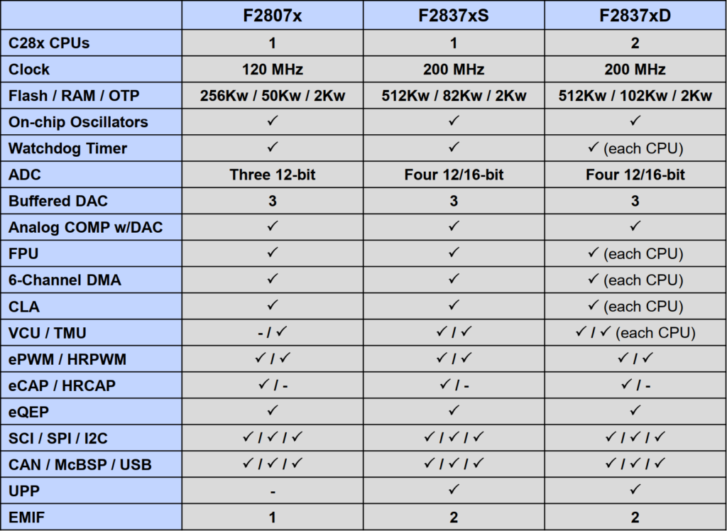
- TMS320F28x7x Device Comparison
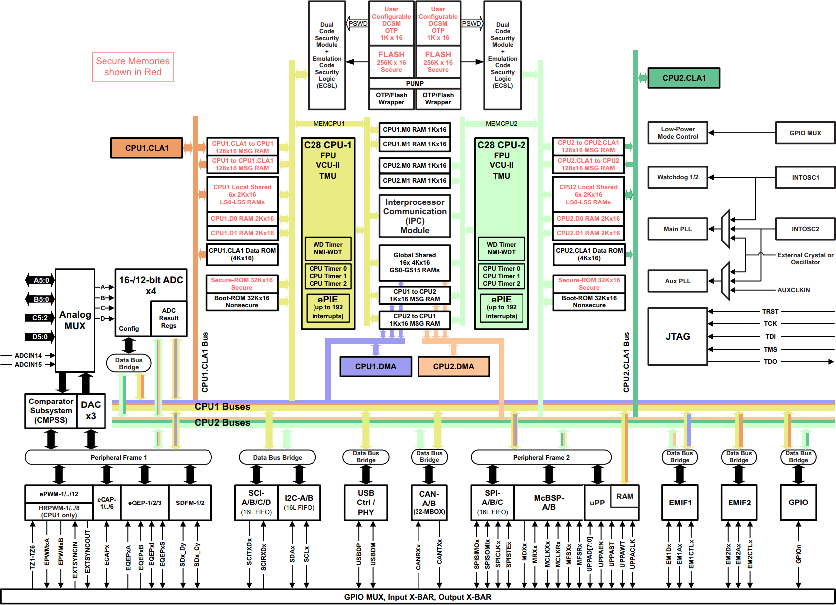
- TMS320F2837xD/F2838xD Dual-Core Block Diagram
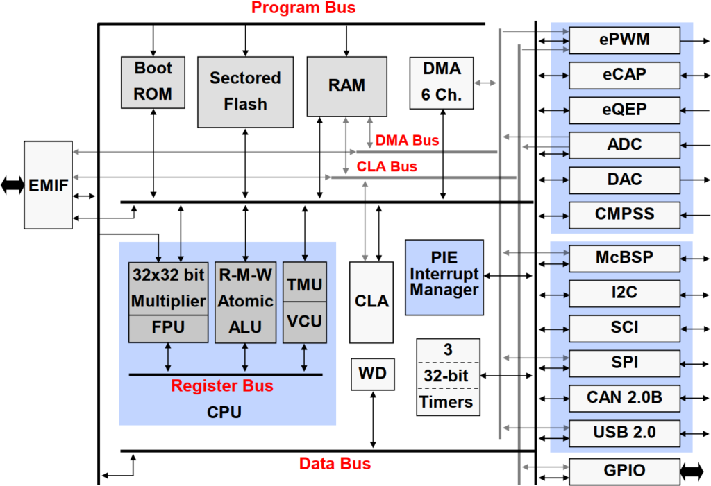
- TMS320F28x7x Core Block Diagram
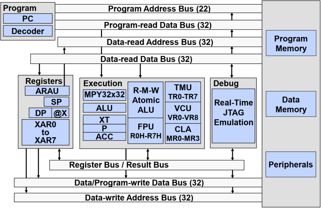
- TMS320F28x7x CPU Internal Bus Structure
- TMS320F28x7x CPU Pipeline
- Math Accelerators: Viterbi / Complex Math Unit (VCU-II)
- Math Accelerators: Trigonometric Math Unit (TMU)
The TI C2000 is ideal for applications combining digital signal processing, microcontroller processing, efficient C code execution, and operating system tasks.
The F2837xD dual-core MCU design is based on the TI 32-bit C28x CPU architecture. Each core is identical with access to its own local RAM and flash memory, as well as globally shared RAM memory. Sharing information between the two CPU cores is accomplished with an Inter-Processor Communications (IPC) module. Additionally, each core shares access to a common set of highly integrated analog and control peripherals, providing a complete solution for demanding real-time high-performance signal processing applications, such as digital power, industrial drives, inverters, and motor control.
The F28x7x device is designed around a multibus architecture, also known as a modified Harvard architecture. This can be seen in the block diagram by the separate program bus and data bus, along with the link between the two buses. This type of architecture greatly enhances the performance of the device.
In the upper left area of the block diagram is the memory section, which consists of the boot ROM, sectored flash, and RAM. Also, notice that the six-channel DMA has its own set of buses.
In the lower left area of the block diagram is the execution section, which consists of a 32-bit by 32-bit hardware multiplier, a read-modify-write atomic ALU, a floating-point unit, a trigonometric math unit, and a Viterbi complex math CRC unit. The control law accelerator (CLA) is an independent and separate unit that has its own set of buses.
The peripherals are grouped on the right side of the block diagram. The upper set is the control peripherals, which consists of the ePWM, eCAP, eQEP, and ADC. The lower set is the communication peripherals and consists of the multichannel buffered serial port, I2C, SCI, SPI, CAN, and USB.
The PIE block, or Peripheral Interrupt Expansion block, manages the interrupts from the peripherals. In the bottom right corner is the general-purpose I/O. The CPU has a watchdog module and three 32-bit general-purpose timers are available. Also, the device features an external memory interface, as shown on the left side.
As with many high performance microcontrollers, multiple busses are used to move data between the memory blocks, peripherals, and the CPU. The C28x memory bus architecture consists of six buses (three address and three data):
- A program read bus (22-bit address line and 32-bit data line)
- A data read bus (32-bit address line and 32-bit data line)
- A data write bus (32-bit address line and 32-bit data line)
The 32-bit-wide data busses provide single cycle 32-bit operations. This multiple bus architecture (Harvard Bus Architecture) enables the C28x to fetch an instruction, read a data value and write a data value in a single cycle. All peripherals and memory blocks are attached to the memory bus with prioritized memory accesses.
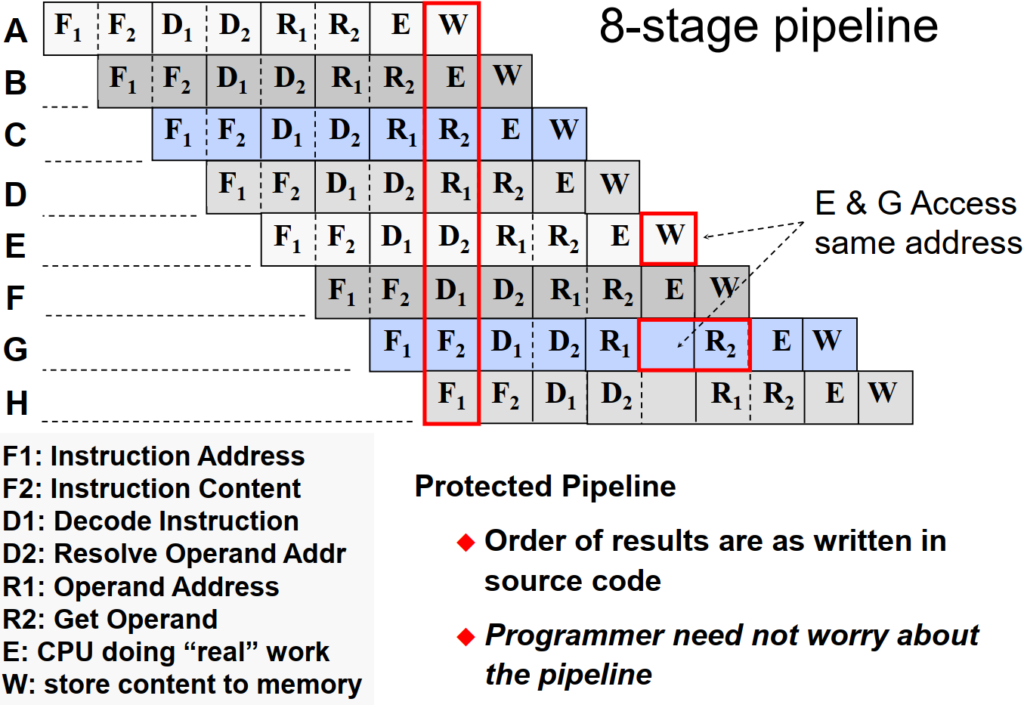
The C28x uses a special 8-stage protected pipeline to maximize the throughput. This protected pipeline prevents a write to and a read from the same location from occurring out of order. This pipelining also enables the C28x CPU to execute at high speeds without resorting to expensive high-speed memories. Special branch-look-ahead hardware minimizes the latency for conditional discontinuities. Special store conditional operations further improve performance. With the 8-stage pipeline most operations can be performed in a single cycle.
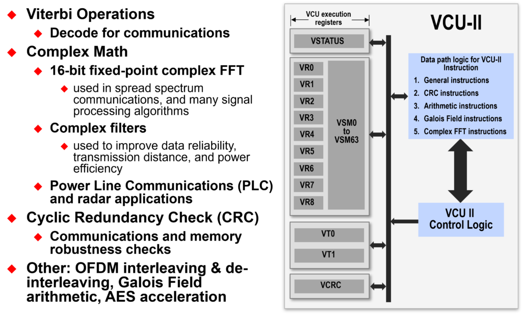
Math Accelerators: Viterbi / Complex Math Unit (VCU-II)
The Viterbi, Complex Math, and CRC Unit (VCU) adds an extended set of registers and instructions to the standard C28x architecture for supporting various communications-based algorithms, such as power line communications (PLC) standards PRIME and G3. These algorithms typically require Viterbi decoding, complex Fast Fourier Transform (FFT), complex filters, and cyclical redundancy check (CRC). By utilizing the VCU a significant performance benefit is realized over a software implementation. It performs fixed-point operations using the existing instruction set format, pipeline, and memory bus architecture. Additionally, the VCU is very useful for general-purpose signal processing applications such as filtering and spectral analysis.
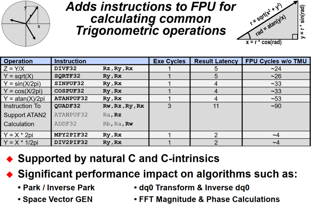
The Trigonometric Math Unit (TMU) is an extension of the FPU and the C28x instruction set, and it efficiently executes trigonometric and arithmetic operations commonly found in control system applications. Similar to the FPU, the TMU provides hardware support for IEEE-754 single precision floating-point operations that are specifically focused on trigonometric math functions. Seamless code integration is accomplished by built-in compiler support that automatically generates TMU instructions where applicable. This dramatically increases the performance of trigonometric functions, which would otherwise be very cycle intensive. It uses the same pipeline, memory bus architecture, and FPU registers as the FPU, thereby removing any special requirements for interrupt context save or restore.
Back to top of the page