
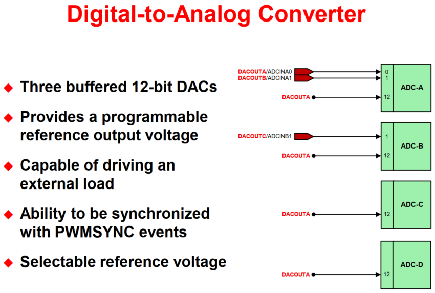
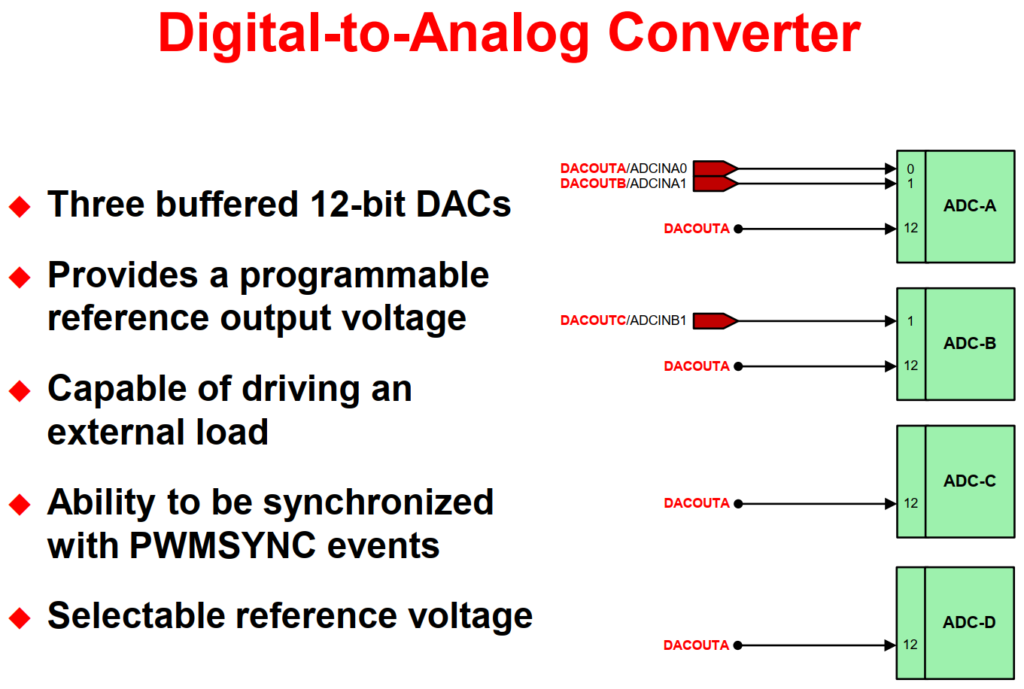
Digital-to-Analog Converter (DAC)
The F2837xD includes three buffered 12-bit DAC modules that can provide a programmable reference output voltage capable of driving an external load. Values written to the DAC can take effect immediately or be synchronized with ePWM events.
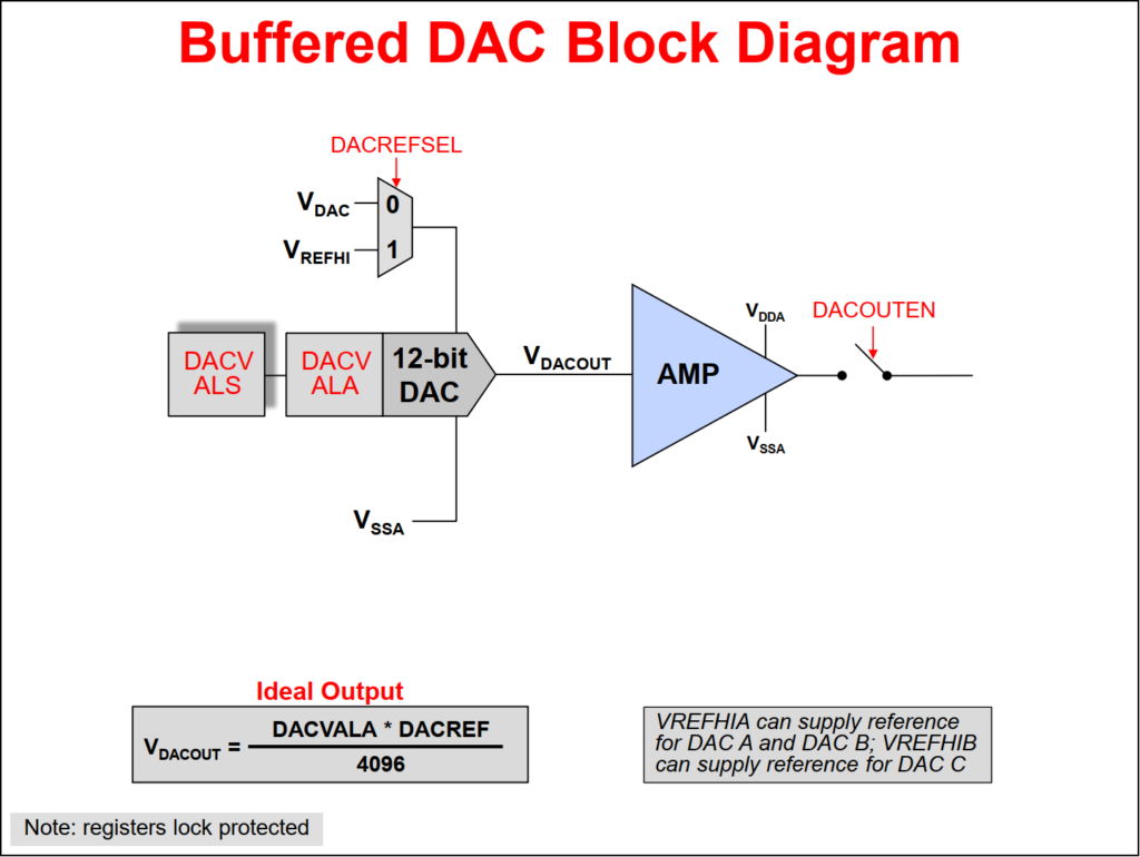
Buffered DAC Block Diagram
Two sets of DACVAL registers are present in the buffered DAC module: DACVALA and DACVALS. DACVALA is a read-only register that actively controls the DAC value. DACVALS is a writable shadow register that loads into DACVALA either immediately or synchronized with the next PWMSYNC event. The ideal output of the internal DAC can be calculated as shown in the equation below.
Example: DACOUTB
void init_DACOUTB(void)
{
    EALLOW;

    // Update the DAC output on the next SYSCLK
    DacbRegs.DACCTL.bit.LOADMODE = 0;

    // Use ADC VREFHI as the DAC reference
    DacbRegs.DACCTL.bit.DACREFSEL = 1;

    // Set DAC-B to mid-scale: 2048 out of 4095
    // Initial value is about 3V/2 = 1.5V
    DacbRegs.DACVALS.all = 0x0800;

    // Enable the DAC-B output buffer
    DacbRegs.DACOUTEN.bit.DACOUTEN = 1;

    EDIS;

    // Wait for the DAC output buffer to power up
    DELAY_US(1000U);

}

Uint16 dacOutput = 1024; // Vref=3, output is about 0.75V
DacbRegs.DACVALS.all = dacOutput;
Reference
Back to top of the page