
- TMS320F28x7x ADC Subsystem
- TMS320F28x7x ADC Module Block Diagram
- TMS320F28x7x ADC SOCx Functional Diagram
- TMS320F28x7x ADC Triggering
- TMS320F28x7x ADC Ping-Pong Triggering
-
TMS320F28x7x ADC Conversion Priority
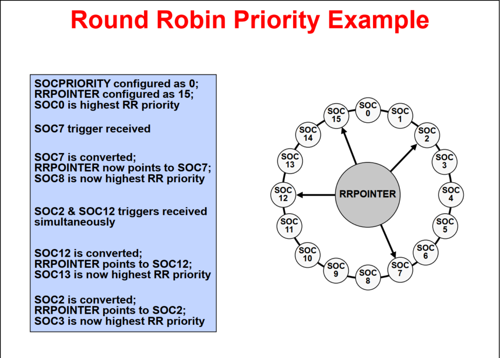
- Example – Round Robin Priority
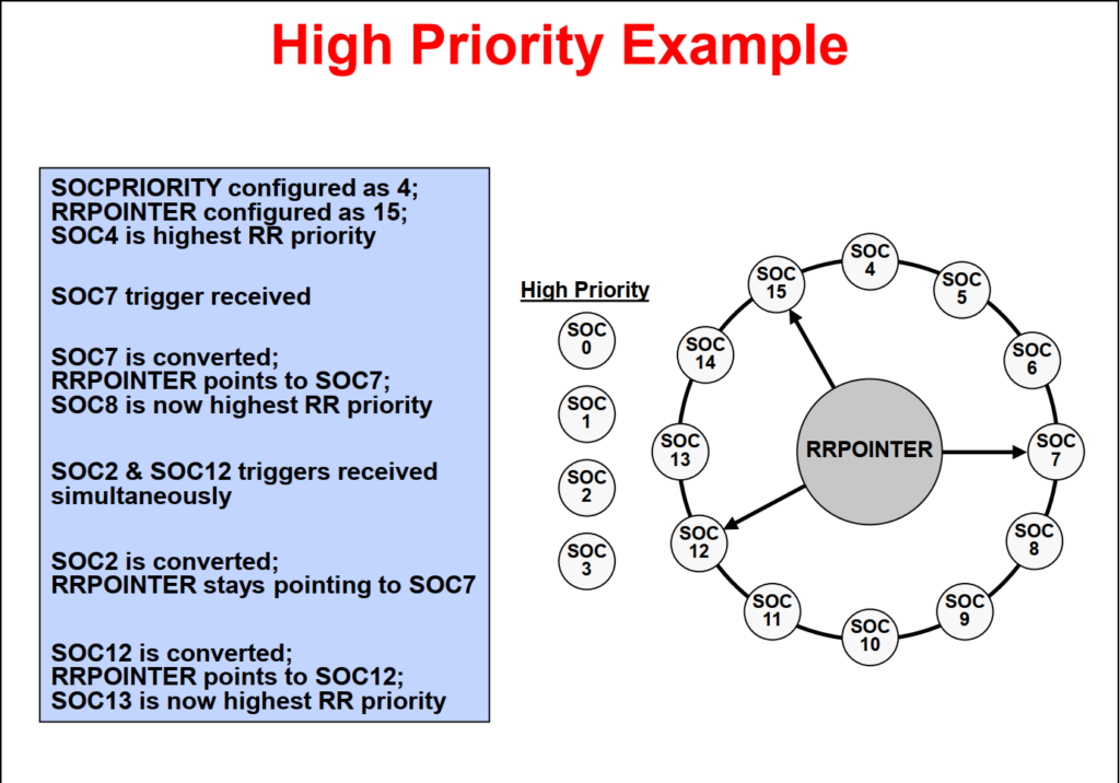
- Example – High Priority
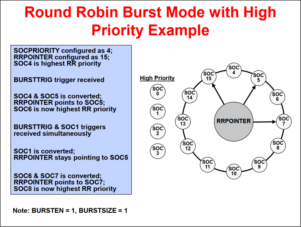
- Example – Round Robin Burst Mode with High Priority
- TMS320F28x7x ADC Post Processing Block
- TMS320F28x7x ADC Clocking Flow
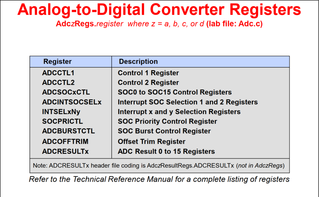
- TMS320F28x7x ADC Converter Registers
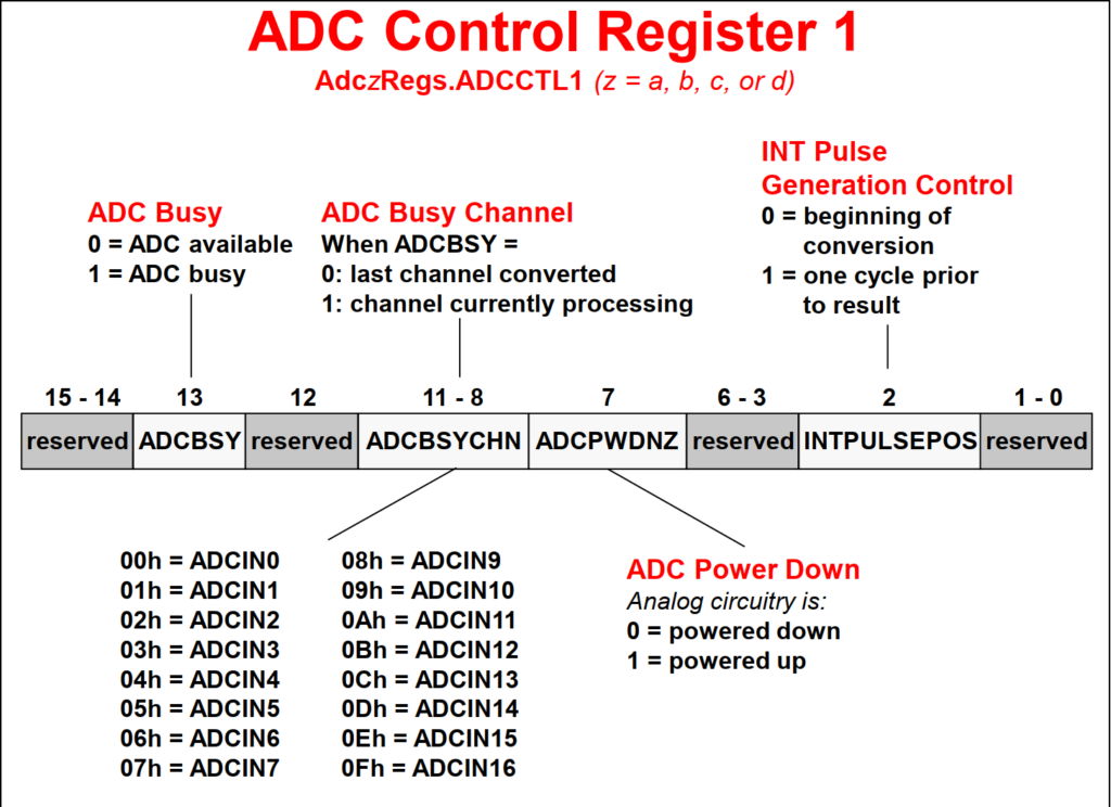
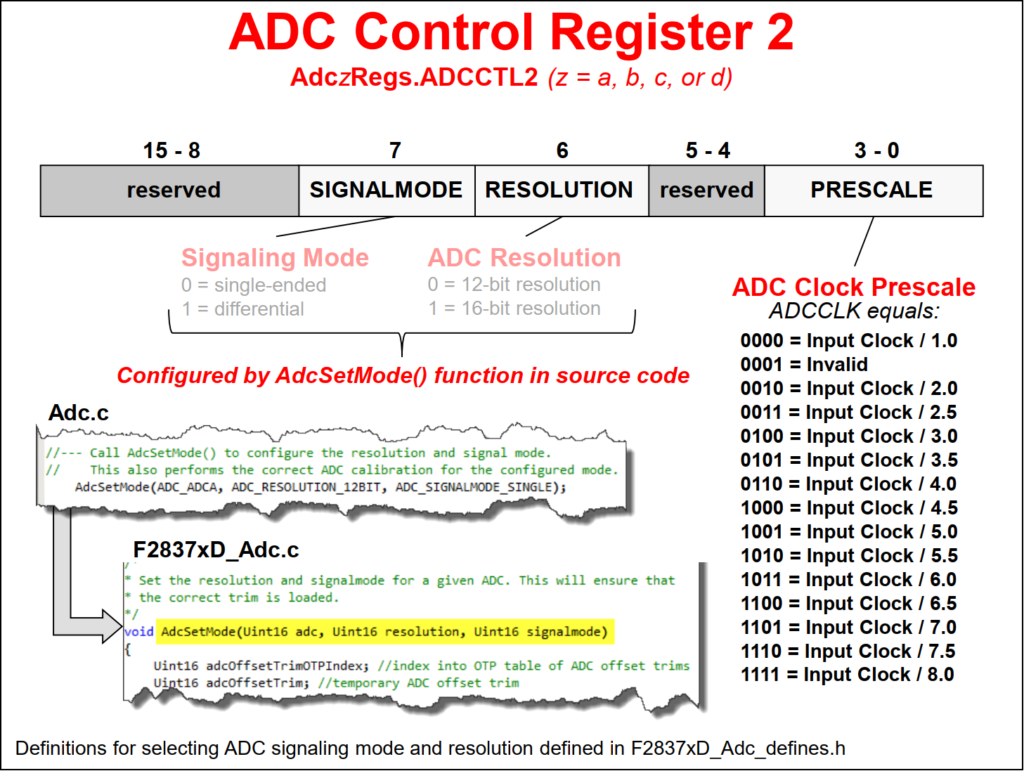
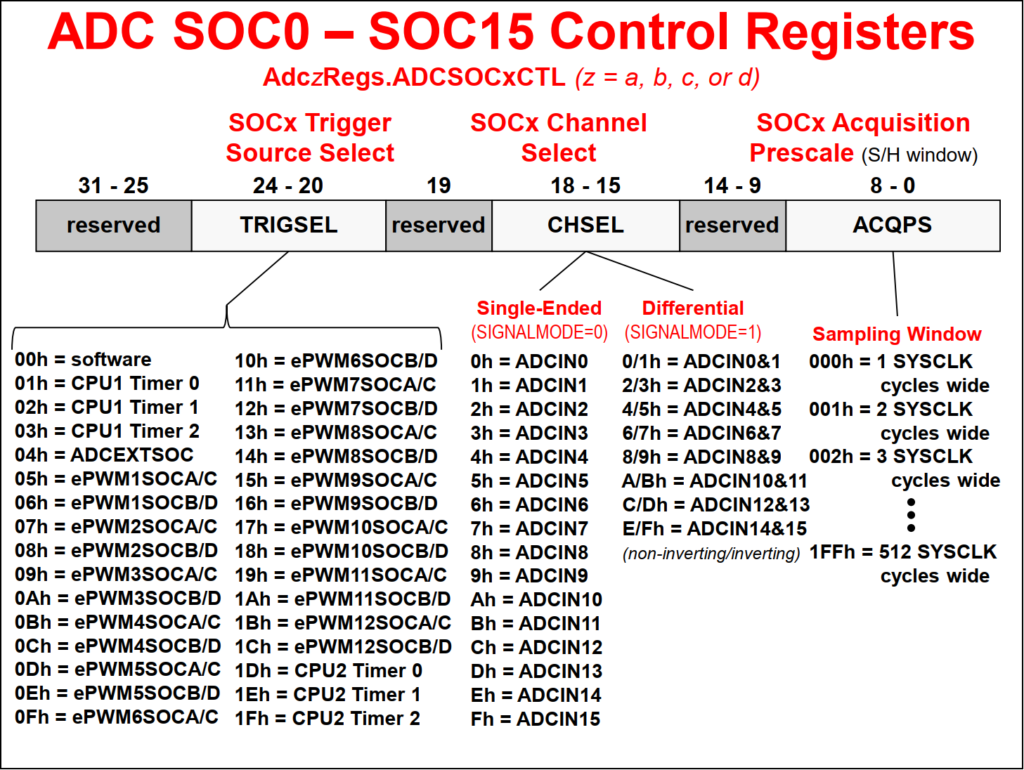
- TMS320F28x7x ADC Control Registers
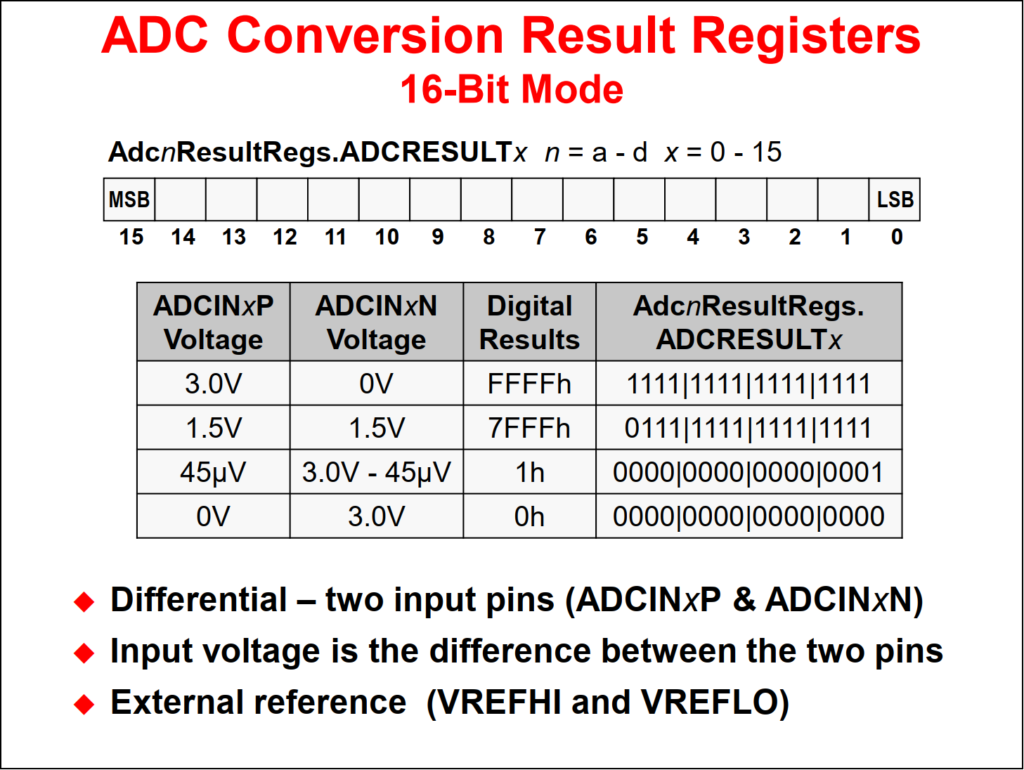
- TMS320F28x7x ADC Conversion Result Registers
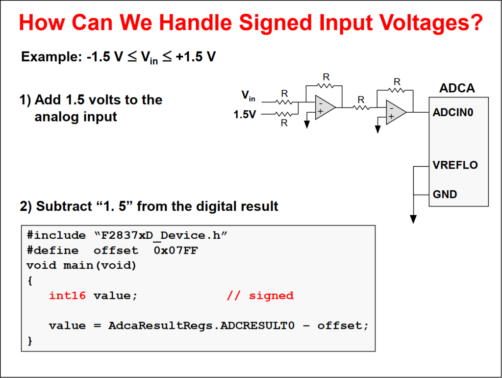
- TMS320F28x7x ADC Signed Input Voltages
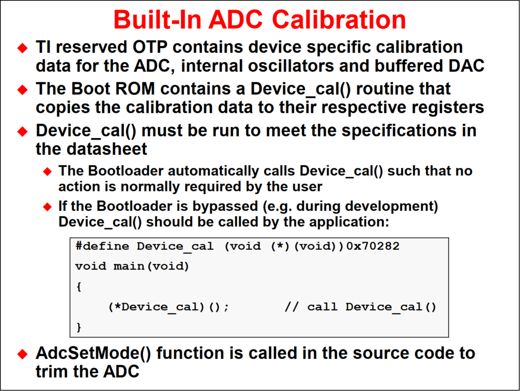
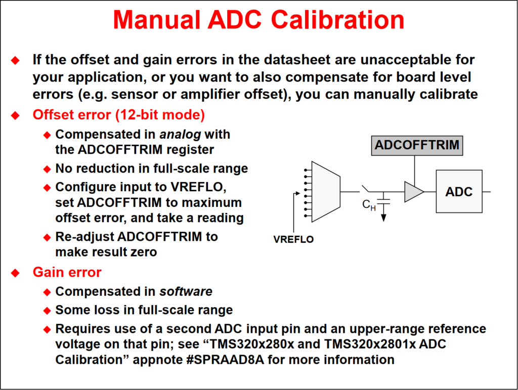
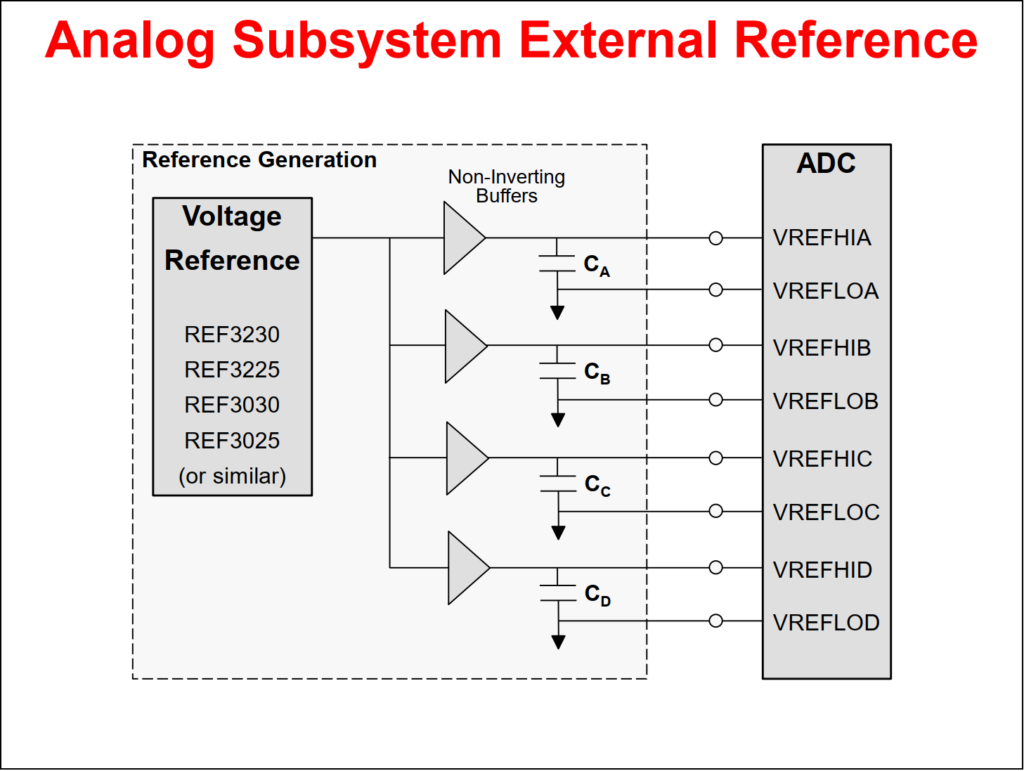
- TMS320F28x7x ADC Calibration and Reference
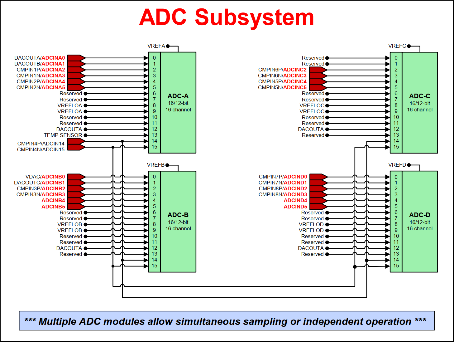
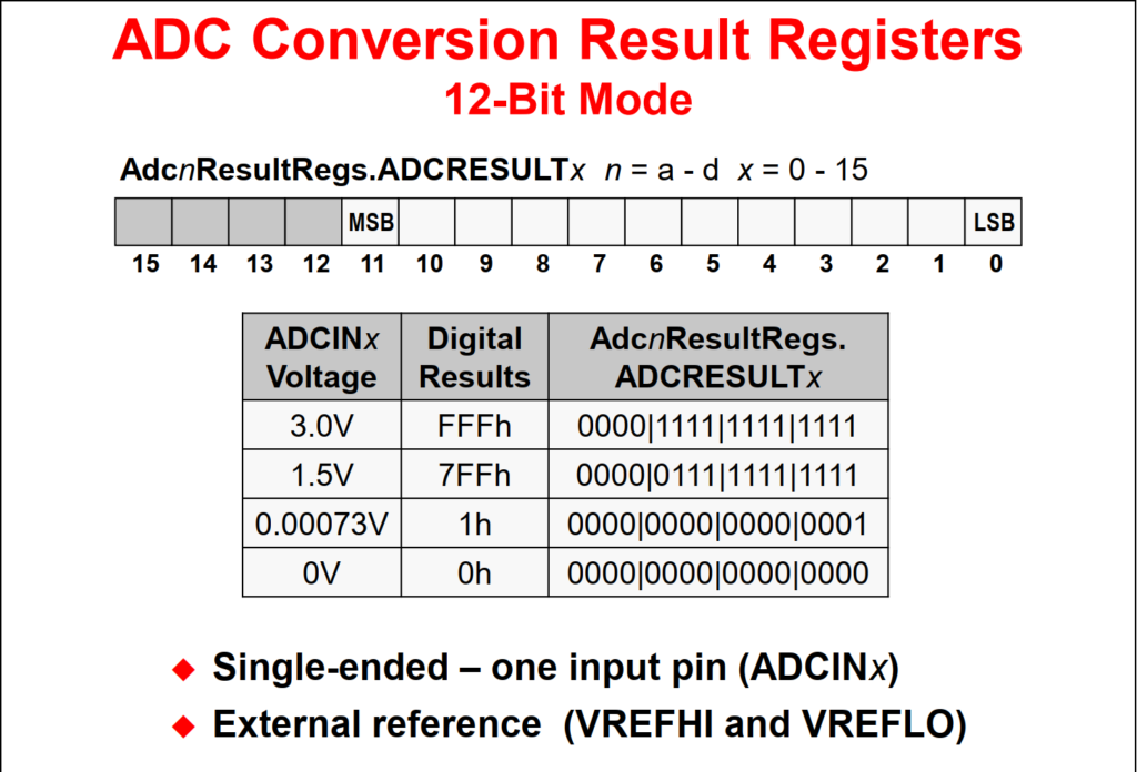
The F2837xD includes four independent high-performance ADC modules which can be accessed by both CPU subsystems, allowing the device to efficiently manage multiple analog signals for enhanced overall system throughput. Each ADC module has a single sample-and-hold (S/H) circuit and using multiple ADC modules enables simultaneous sampling or sequential sampling. The ADC module is implemented using a successive approximation (SAR) type ADC with a configurable resolution of either 16-bits or 12-bits.
For 16-bit resolution, the ADC performs differential signal conversions with a performance of 1.1 MSPS, yielding 4.4 MSPS for the device. In differential signal mode, a pair of pins (positive input ADCINxP and negative input ADCINxN) is sampled and the input applied to the converter is the difference between the two pins (ADCINxP – ADCINxN). A benefit of differential signaling mode is the ability to cancel noise that may be introduced common to both inputs. For 12-bit resolution, the ADC performs single-ended signal conversions with a performance of 3.5 MSPS, yielding 14 MSPS for the device. In single-ended mode, a single pin (ADCINx) is sampled and applied to the input of the converter.

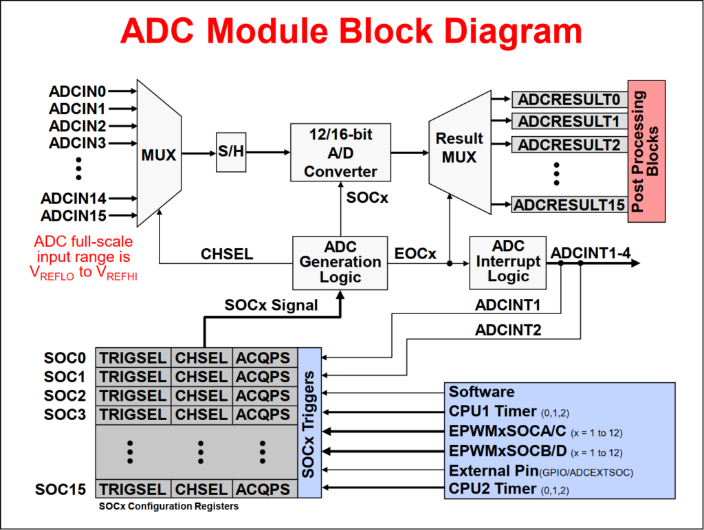
The ADC triggering and conversion sequencing is managed by a series of start-of-conversion (SOCx) configuration registers. Each SOCx register configures a single channel conversion, where the SOCx register specifies the trigger source that starts the conversion, the channel to convert, and the acquisition sample window duration. Multiple SOCx registers can be configured for the same trigger, channel, and/or acquisition window. Configuring multiple SOCx registers to use the same trigger will cause that trigger to perform a sequence of conversions, and configuring multiple SOCx registers for the same trigger and channel can be used to oversample the signal.
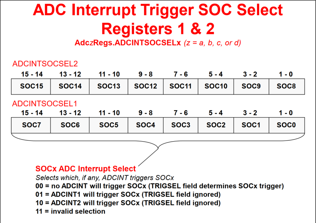
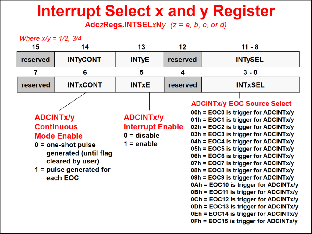
The various trigger sources that can be used to start an ADC conversion include the General Purpose Timers from each CPU subsystem, the ePWM modules, an external pin, and by software. Also, the flag setting of either ADCINT1 or ADCINT2 can be configured as a trigger source which can be used for continuous conversion operation. The ADC interrupt logic can generate up to four interrupts. The results for SOC 0 through 15 appear in result registers 0 through 15, respectively.
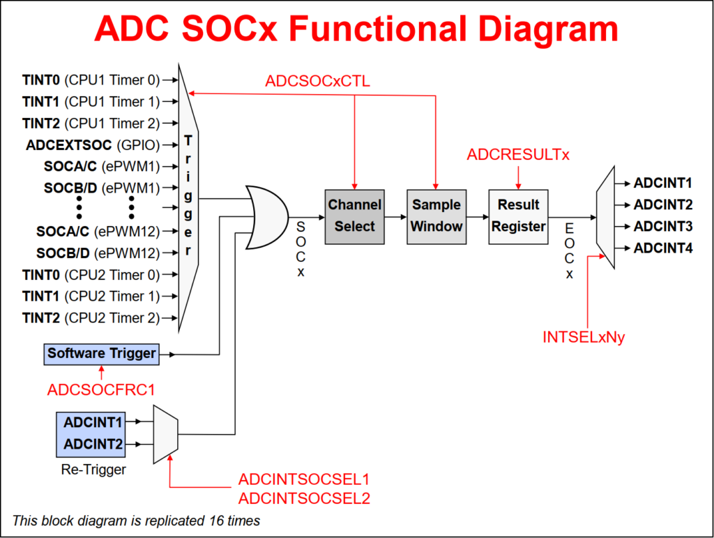
The figure below is a conceptual view highlighting a single ADC start-of-conversion (SOC) functional flow from triggering to interrupt generation. This figure is replicated 16 times and the red text indicates the register names.
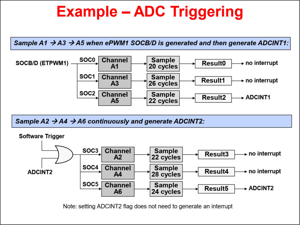
The top example in the figure below shows channels A1, A3, and A5 being converted with a trigger from EPWM1. After A5 is converted, ADCINT1 is generated. The bottom example shows channels A2, A4, and A6 being converted initially by a software trigger. Then, after A6 is converted, ADCINT2 is generated and also fed back as a trigger to start the process again.
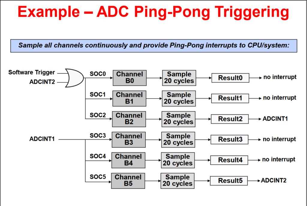
The ADC ping-pong triggering example in the figure below shows channels B0 through B5 being converted, triggered initially by software. After channel B2 is converted, ADCINT1 is generated, which also triggers channel B3. After channel B5 is converted, ADCINT2 is generated and is also fed back to start the process again from the beginning. Additionally, ADCINT1 and ADCINT2 are being used to manage the ping-pong interrupts for the interrupt service routines.
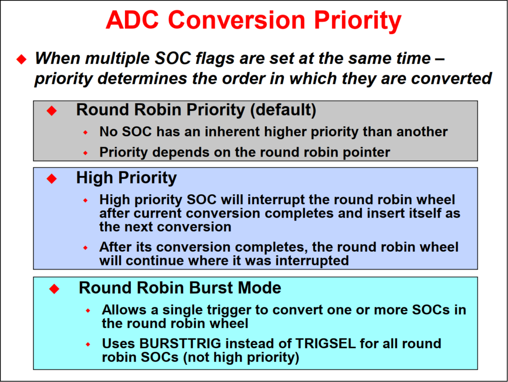
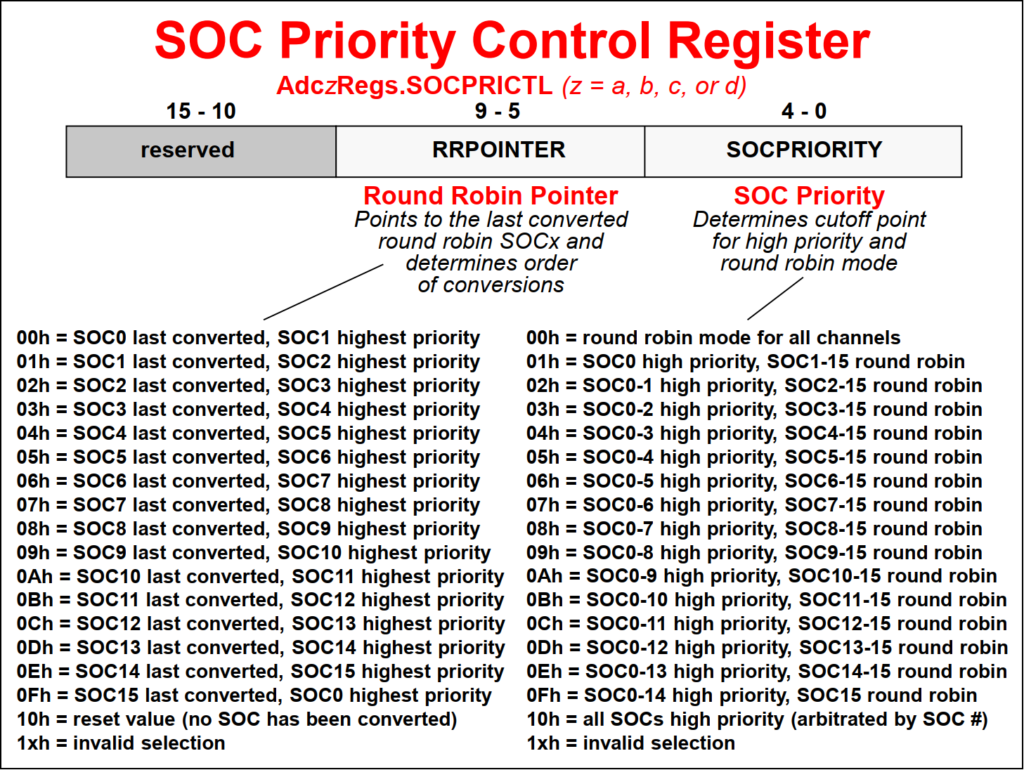
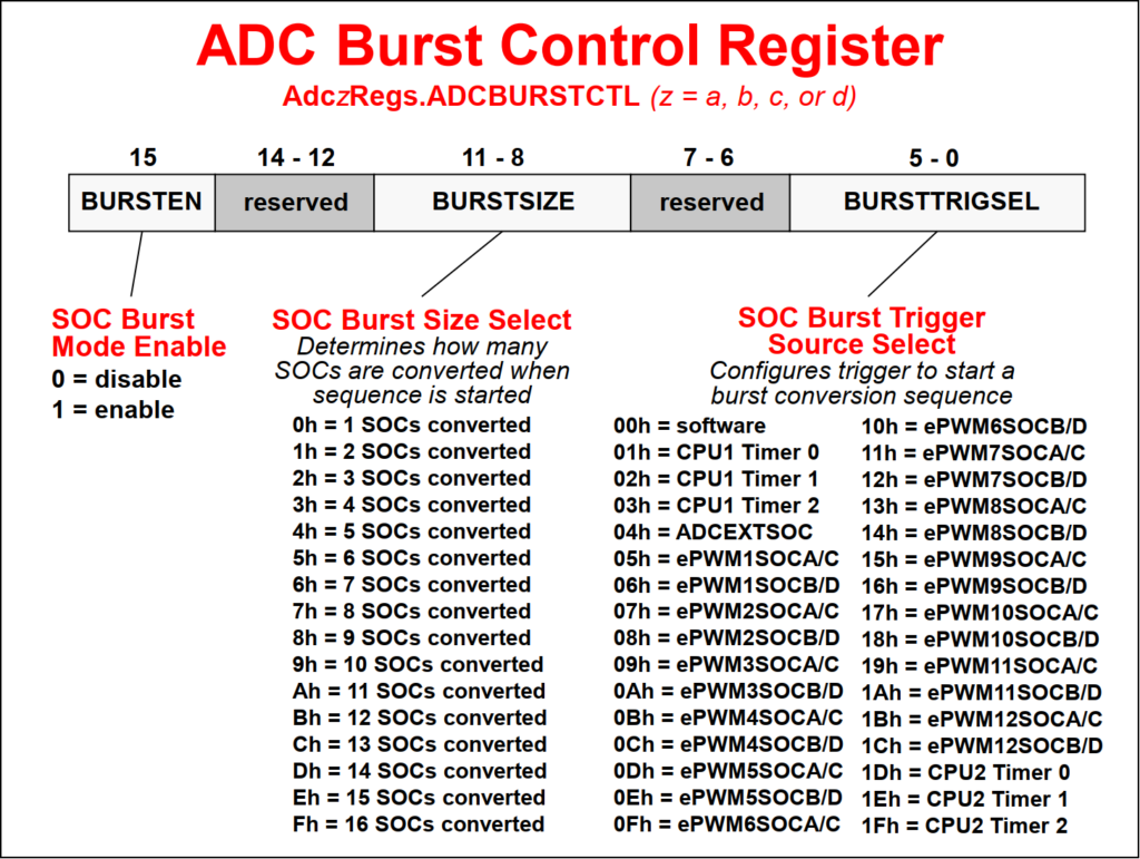
When multiple triggers are received at the same time, the ADC conversion priority determines the order in which they are converted. Three different priority modes are supported. The default priority mode is round robin, where no start-of-conversion has an inherently higher priority over another, and the priority depends upon a round robin pointer. The round robin pointer operates in a circular fashion, constantly wrapping around to the beginning. In high priority mode, one or more than one start-of-conversion is assigned as high priority. The high priority start-of-conversion can then interrupt the round robin wheel, and after it has been converted the wheel will continue where it was interrupted. High priority mode is assigned first to the lower number start-of-conversion and then in increasing numerical order. If two high priority start-of-conversion triggers occur at the same time, the lower number will take precedence. Burst mode allows a single trigger to convert one or more than one start-of-conversion sequentially at a time. This mode uses a separate Burst Control register to select the burst size and trigger source.
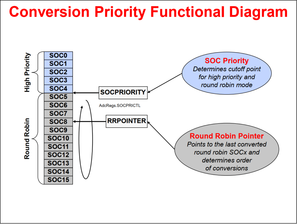
In this conversion priority functional diagram, the Start-of-Conversion Priority Control Register contains two bit fields. The Start-of-Conversion Priority bit fields determine the cutoff point between high priority and round robin mode, whereas the Round-Robin Pointer bit fields contains the last converted round robin start-of-conversion which determines the order of conversions.
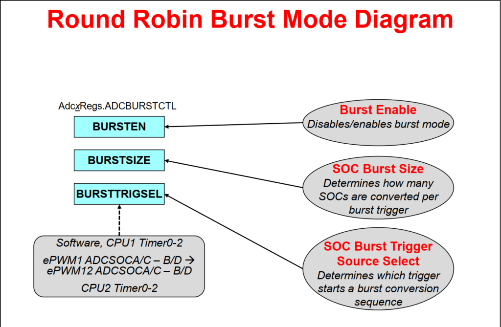
The Round-Robin Burst mode utilizes an ADC Burst Control Register to enable the burst mode, determine the burst size, and select the burst trigger source.
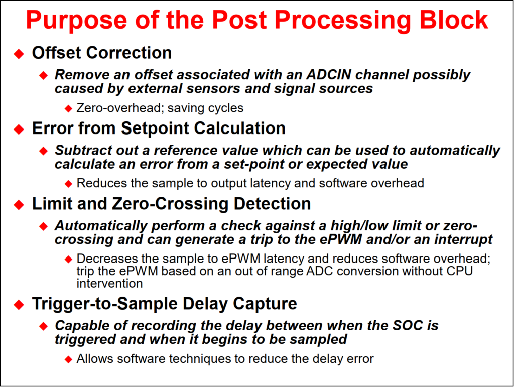
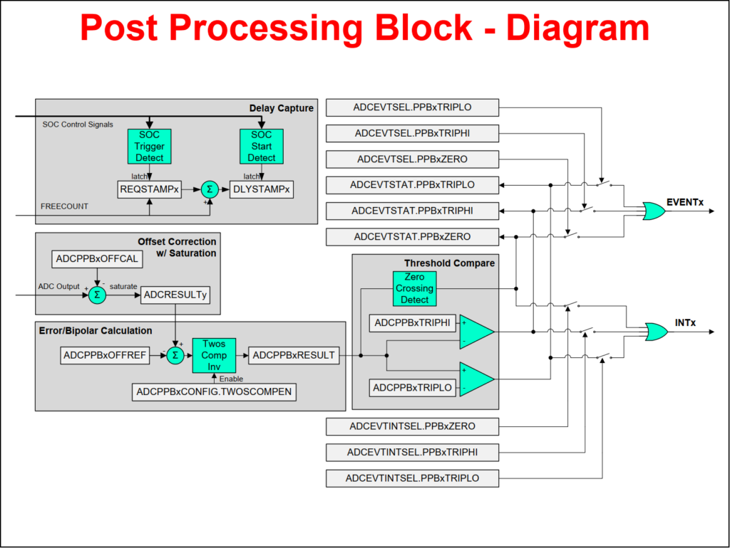
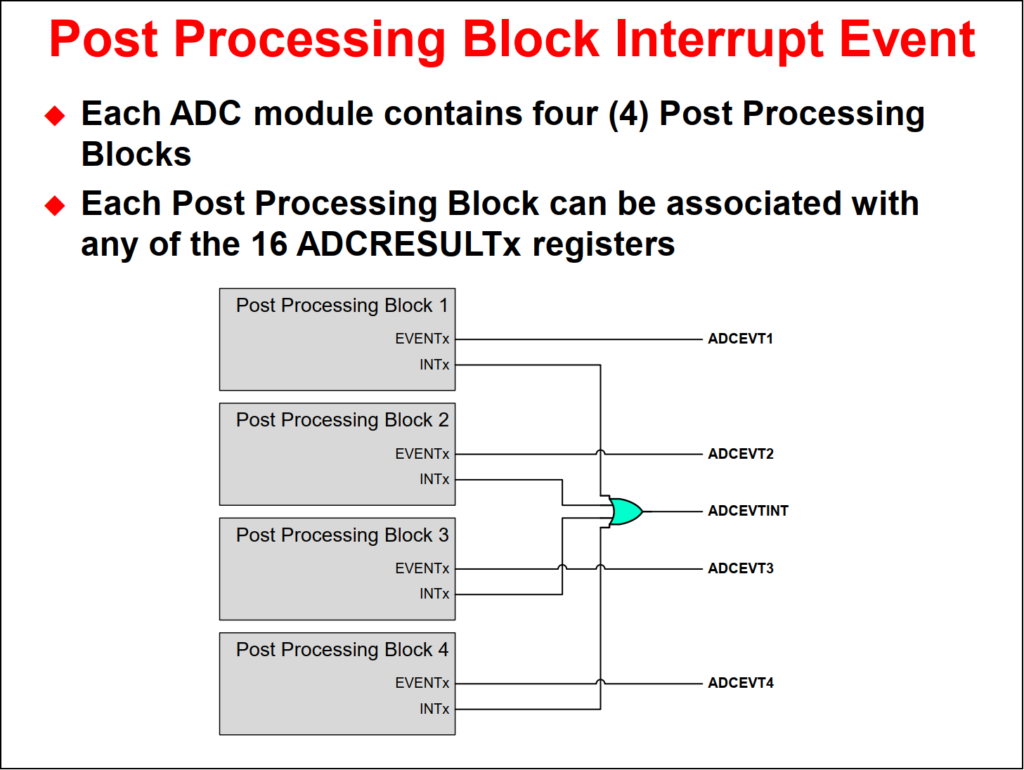
To further enhance the capabilities of the ADC, each ADC module incorporates four postprocessing blocks (PPB), and each PPB can be linked to any of the ADC result registers. The PPBs can be used for offset correction, calculating an error from a set-point, detecting a limit and zero-crossing, and capturing a trigger-to-sample delay.
Offset correction can simultaneously remove an offset associated with an ADCIN channel that was possibly caused by external sensors or signal sources with zero-overhead, thereby saving processor cycles.Error calculation can automatically subtract out a computed error from a set-point or expected result register value, reducing the sample to output latency and software overhead.
Limit and zero-crossing detection automatically performs a check against a high/low limit or zero-crossing and can generate a trip to the ePWM and/or generate an interrupt. This lowers the sample to ePWM latency and reduces software overhead. Also, it can trip the ePWM based on an out-of-range ADC conversion without any CPU intervention which is useful for safety conscious applications.
Sample delay capture records the delay between when the SOCx is triggered and when it begins to be sampled. It can enable software techniques to be used for reducing the delay error.
Back to top of the page