
- TMS320F28x7x Interrupt Sources
- TMS320F28x7x Interrupt Processing
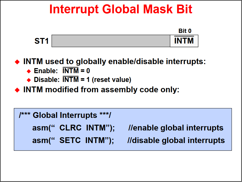
- TMS320F28x7x IFR, IER, INTM
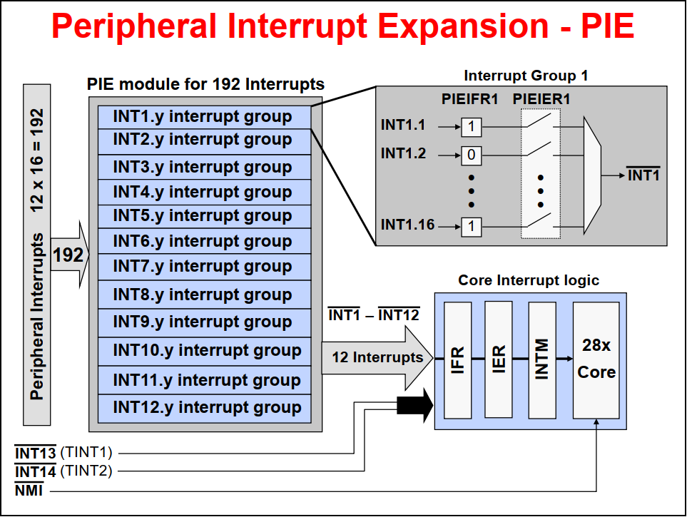
- TMS320F28x7x Peripheral Interrupt Expansion (PIE)
- TMS320F28x7x PIE Block Initialization
- TMS320F28x7x Interrupt Signal Flow
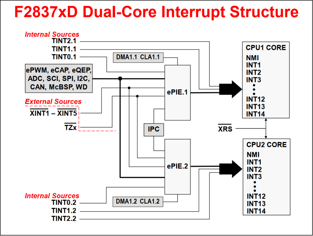
- TMS320F28x7D Dual-Core Interrupt Structure
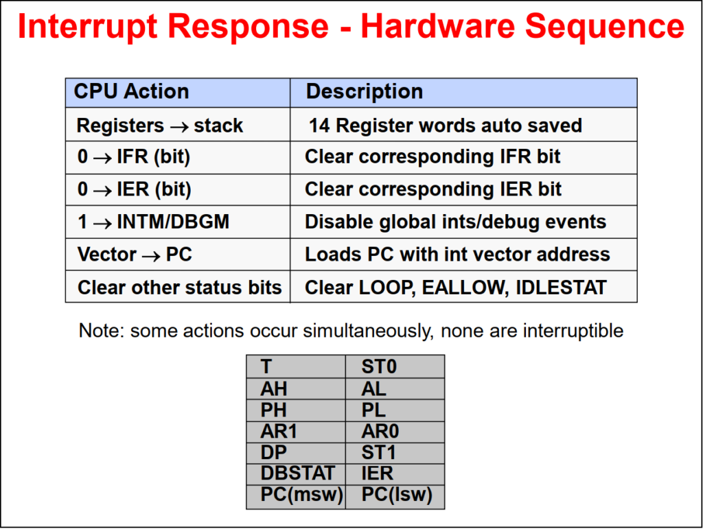
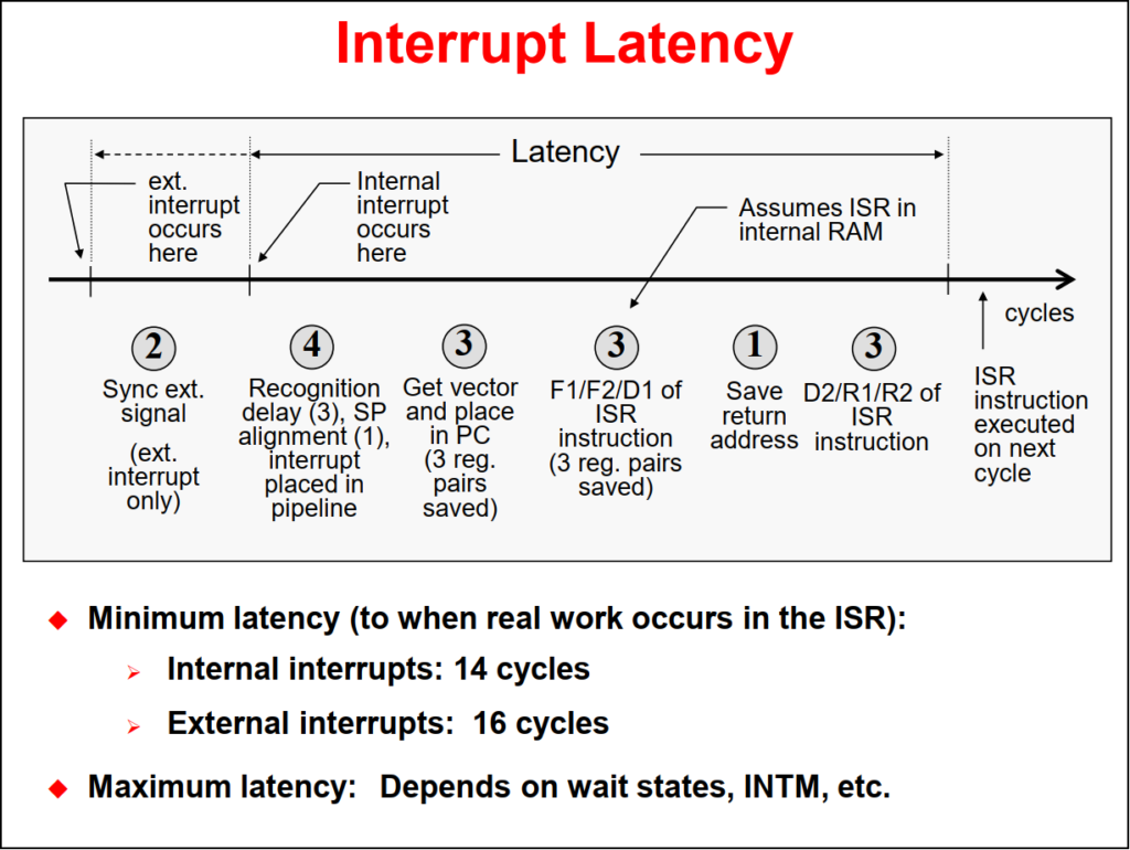
- TMS320F28x7x Interrupt Response and Latency
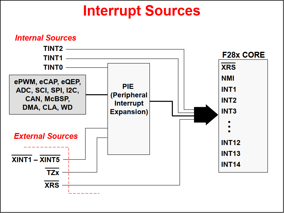
The internal interrupt sources include the general purpose timers 0, 1, and 2, and all of the peripherals on the device. External interrupt sources include the three external interrupt lines, the trip zones, and the external reset pin. The core has 14 interrupt lines. The Peripheral Interrupt Expansion block, known as the PIE block, is connected to the core interrupt lines 1 through 12 and is used to expand the core interrupt capability, allowing up to 192 possible interrupt sources.
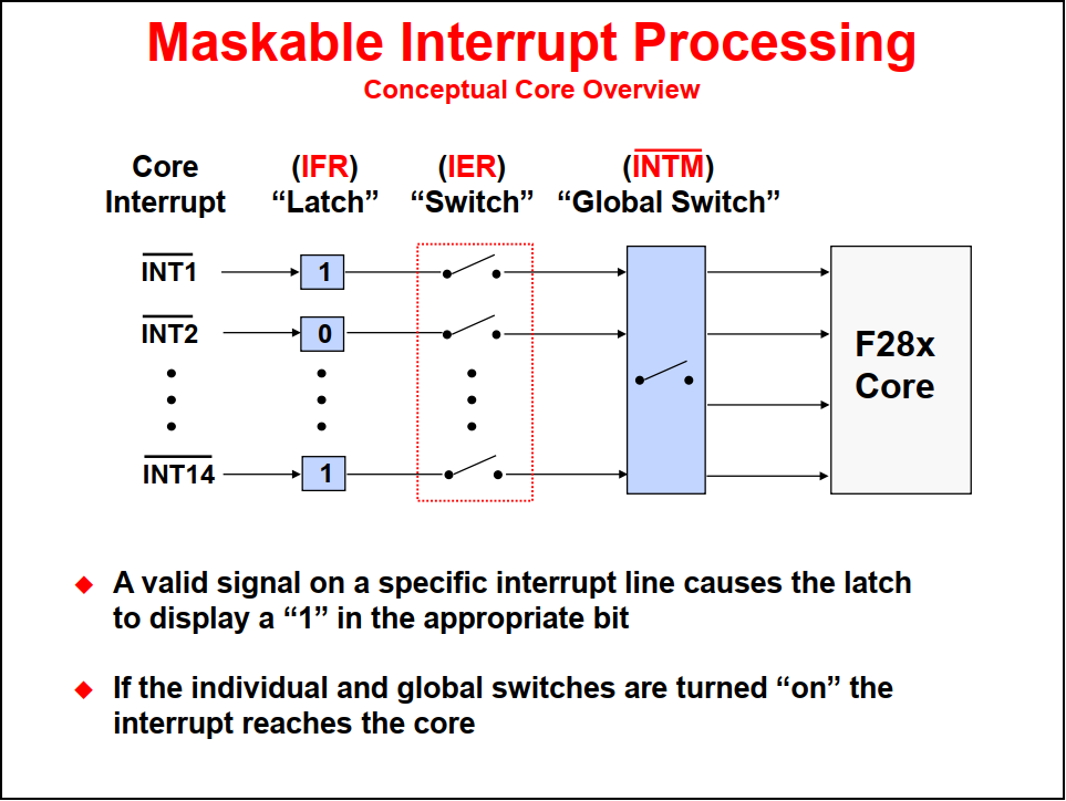
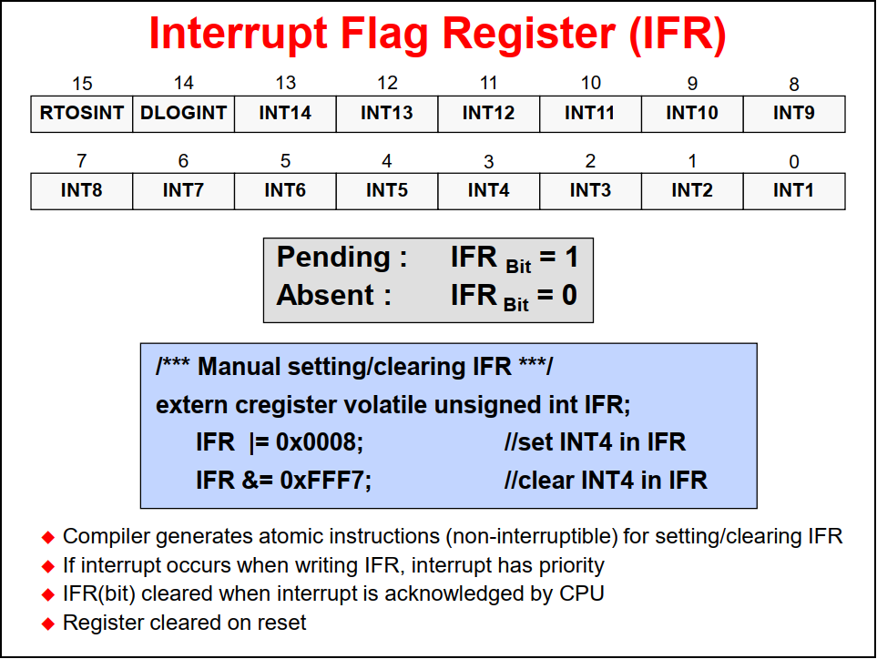
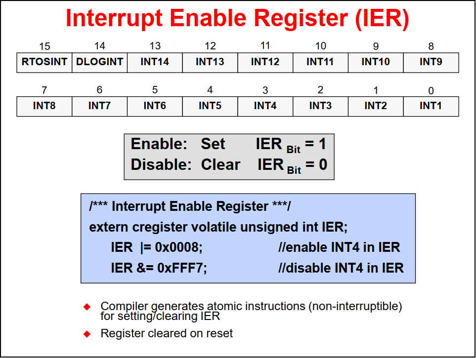
By using a series of flag and enable registers, the CPU can be configured to service one interrupt while others remain pending, or perhaps disabled when servicing certain critical tasks. When an interrupt signal occurs on a core line, the interrupt flag register (IFR) for that core line is set. If the appropriate interrupt enable register (IER) is enabled for that core line, and the interrupt global mask (INTM) is enabled, the interrupt signal will propagate to the core.
Once the interrupt service routine (ISR) starts processing the interrupt, the INTM bit is disabled to prevent nested interrupts. The IFR is then cleared and ready for the next interrupt signal. When the interrupt servicing is completed, the INTM bit is automatically enabled, allowing the next interrupt to be serviced. Notice that when the INTM bit is 0, the switch is closed and enabled. When the bit is 1, the switch is open and disabled. The IER is managed by ORing and ANDing mask values. The INTM bit in the status register is managed by using in-line assembly instructions.
// Disable CPU interrupts
DINT;

// Disable CPU interrupts and clear all CPU interrupt flags
IER = 0x0000;
IFR = 0x0000;

// Enable global Interrupts and higher priority real-time debug events
EINT; // Enable Global interrupt INTM
ERTM; // Enable Global real-time interrupt DBGMThe C28x CPU core has a total of fourteen interrupt lines, of which two interrupt lines are directly connected to CPU Timers 1 and 2 (on INT13 and INT14, respectively) and the remaining twelve interrupt lines (INT1 through INT12) are used to service the peripheral interrupts. A Peripheral Interrupt Expansion (PIE) module multiplexes up to sixteen peripheral interrupts into each of the twelve CPU interrupt lines, further expanding support for up to 192 peripheral interrupt signals. The PIE module also expands the interrupt vector table, allowing each unique interrupt signal to have its own interrupt service routine (ISR), permitting the CPU to support a large number of peripherals.
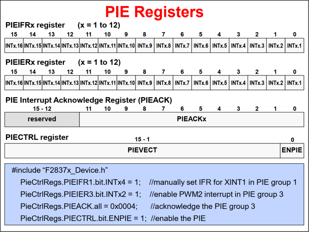
The PIE module has an individual flag and enable bit for each peripheral interrupt signal. Each of the sixteen peripheral interrupt signals that are multiplexed into a single CPU interrupt line is referred to as a group, so the PIE module consists of 12 groups. Each PIE group has a 16-bit flag register (PIEIFRx), a 16-bit enable register (PIEIERx), and a bit field in the PIE acknowledge register (PIEACK) which acts as a common interrupt mask for the entire group.
For a peripheral interrupt to propagate to the CPU, the appropriate PIEIFR must be set, the PIEIER enabled, the CPU IFR set, the IER enabled, and the INTM enabled. Note that some peripherals can have multiple events trigger the same interrupt signal, and the cause of the interrupt can be determined by reading the peripheral’s status register.
We have already discussed the interrupt process in the core. Now we need to look at the peripheral interrupt expansion block. This block is connected to the core interrupt lines 1 through 12. The PIE block consists of 12 groups. Within each group, there are sixteen interrupt sources. Each group has a PIE interrupt enable register and a PIE interrupt flag register. Note that interrupt lines 13, 14, and NMI bypass the PIE block.
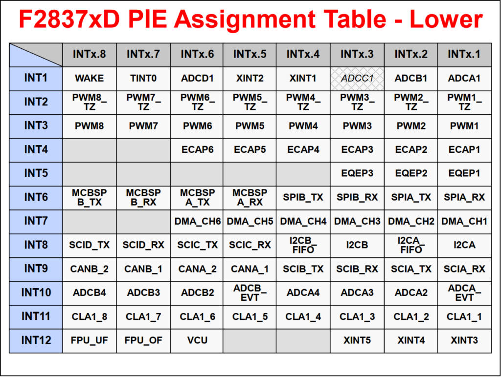
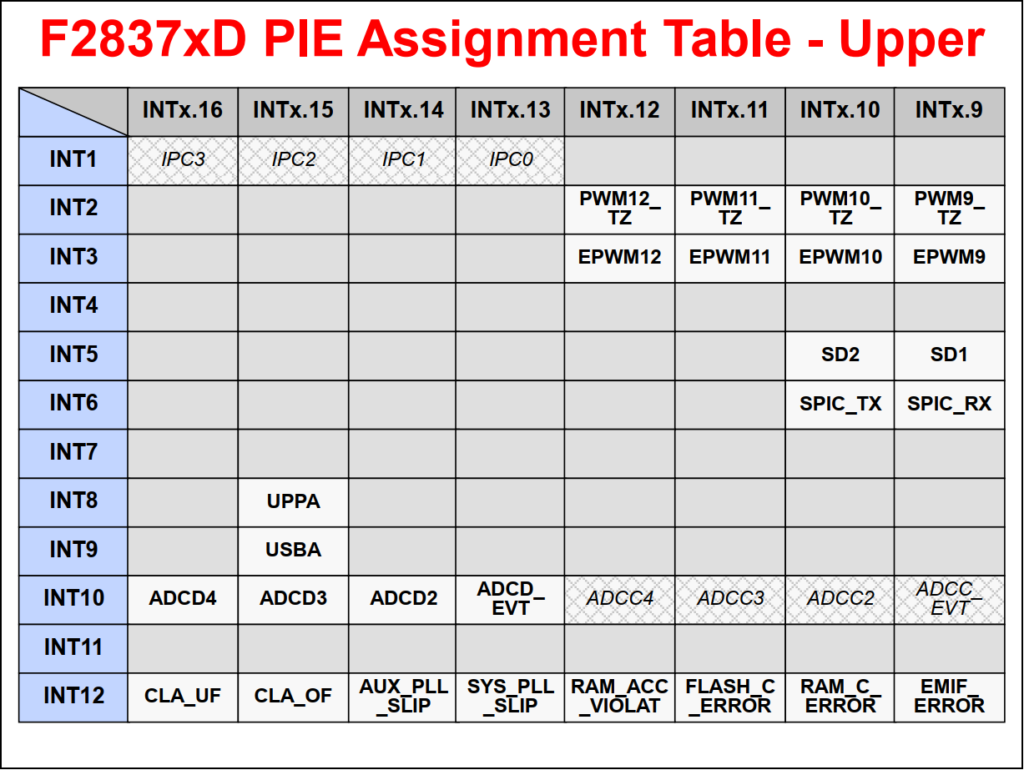
The PIE assignment table maps each peripheral interrupt to the unique vector location for that interrupt service routine. Notice the interrupt numbers on the left represent the twelve core group interrupt lines and the interrupt numbers across the top represent the lower eight of the sixteen peripheral interrupts within the core group interrupt line. The next figure shows the upper eight of the sixteen peripheral interrupts within the core group interrupt line.
Similar to the core interrupt process, the PIE module has an individual flag and enable bit for each peripheral interrupt signal. Each PIE group has a 16-bit flag register, a 16-bit enable register, and a bit field in the PIE acknowledge register which acts as a common interrupt mask for the entire group. The enable PIE bit in the PIECTRL register is used to activate the PIE module.
// Clear all interrupts and initialize PIE vector table:
// Disable CPU interrupts
DINT;

// Initialize the PIE control registers to their default state.
// The default state is all PIE interrupts disabled and flags are cleared.
// This function is found in the F2837xD_PieCtrl.c file.
InitPieCtrl();

// Disable CPU interrupts and clear all CPU interrupt flags:
IER = 0x0000;
IFR = 0x0000;

// Initialize the PIE vector table with pointers to the shell
// Interrupt Service Routines (ISR).
// This will populate the entire table, even if the interrupt
// is not used in this example.
// The shell ISR routines are found in F2837xD_DefaultIsr.c.
// This function is found in F2837xD_PieVect.c.
InitPieVectTable();

// Interrupts that are used in this example are re-mapped to
// ISR functions found within this project
EALLOW;
PieVectTable.SCIA_RX_INT = &RXAINT_recv_ready;
PieVectTable.SCIA_TX_INT = &TXAINT_data_sent;
EDIS;

// Enable group 9 for SCIA RX/TX
IER |= (M_INT9);

// Enable SCI-A RX interrupt in the PIE: group 9 channel 1
PieCtrlRegs.PIEIER9.bit.INTx1 = 1;

// Enable SCI-A TX interrupt in the PIE: group 9 channel 2
PieCtrlRegs.PIEIER9.bit.INTx2 = 1;

// Enable global Interrupts and higher priority real-time debug events
EINT;  // Enable Global interrupt INTM
ERTM;  // Enable Global realtime interrupt DBGM

// Called in RX/TX ISR function
// Acknowledge this interrupt to receive more interrupts from group 9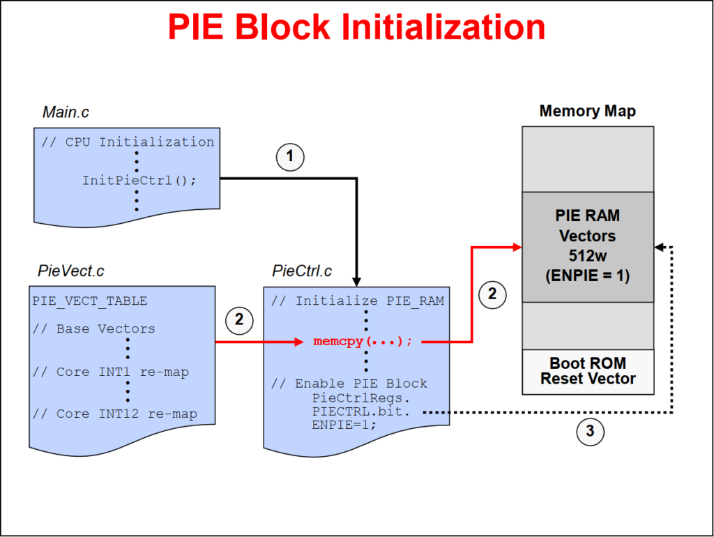
PieCtrlRegs.PIEACK.all = PIEACK_GROUP9;The interrupt vector table, as mapped in the PIE interrupt assignment table, is located in the PieVect.c file. During processor initialization a function call to PieCtrl.c file is used to copy the interrupt vector table to the PIE RAM and then the PIE module is enabled by setting ENPIE to 1. When the CPU receives an interrupt, the vector address of the ISR is fetched from the PIE RAM, and the interrupt with the highest priority that is both flagged and enabled is executed. Priority is determined by the location within the interrupt vector table. The lowest numbered interrupt has the highest priority when multiple interrupts are pending.
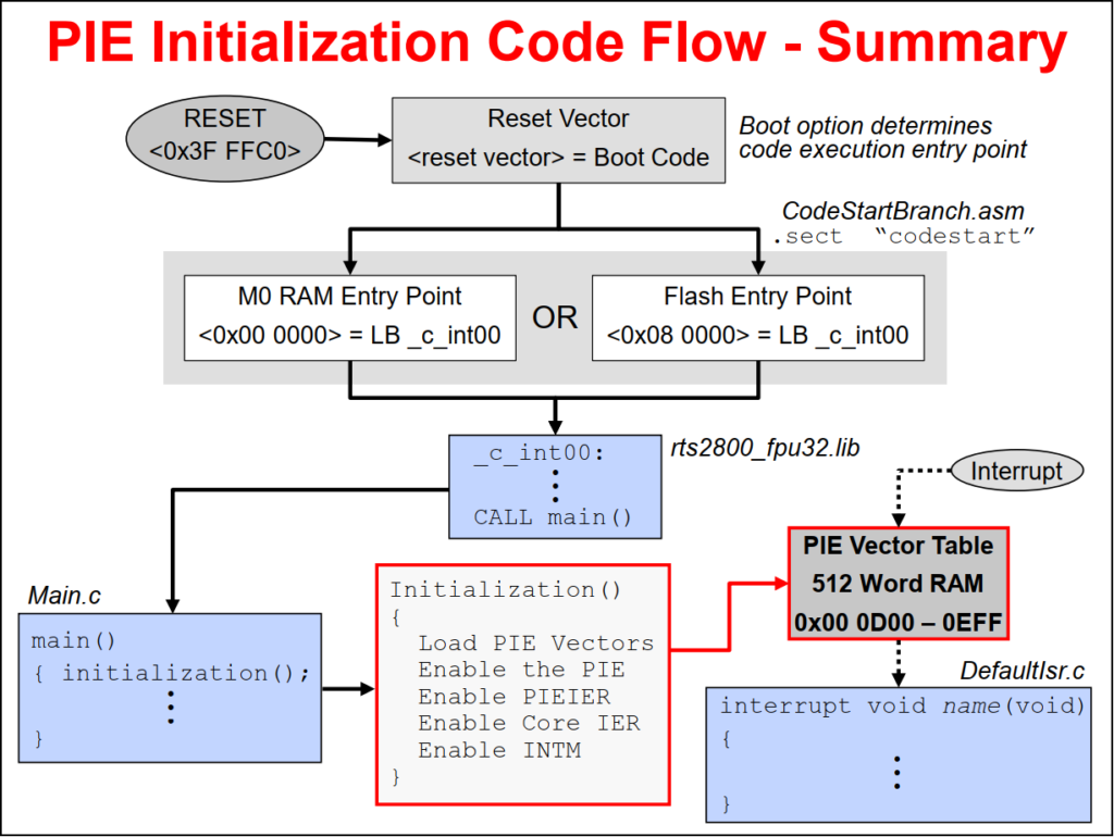
In summary, the PIE initialization code flow is as follows. After the device is reset and execution of the boot code is completed, the selected boot option determines the code entry point. In this figure, two different entry points are shown. The one on the left is for memory block M0 RAM, and the one on the right is for flash.
In either case, the CodeStartBranch.asm file has a Long Branch instruction to the entry point of the runtime support library. After the runtime support library completes execution, main is called. In main, a function is called to initialize the interrupt process and enable the PIE module. When the CPU receives an interrupt, the vector address of the ISR is fetched from the PIE RAM, and the interrupt with the highest priority that is both flagged and enabled is executed. Priority is determined by the location within the interrupt vector table.
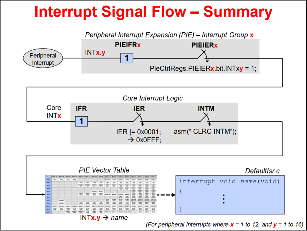
In summary, the following steps occur during an interrupt process. First, a peripheral interrupt is generated and the PIE interrupt flag register is set. If the PIE interrupt enable register is enabled, then the core interrupt flag register will be set. Next, if the core interrupt enable register and global interrupt mask is enabled, the PIE vector table will redirect the code to the interrupt service routine.
Each C28x CPU core in the F2837xD device has its own PIE module, and each PIE module is configured independently. Some interrupt signals are sourced from shared peripherals that canbe owned by either CPU, and these interrupt signals are sent to both CPU PIE modules regardless of which CPU owns the peripheral. Therefore, if enabled a peripheral owned by one CPU can cause an interrupt on the other CPU.
Back to top of the page