
- TMS320F28x7x Memory Map
- TMS320F2837xD Memory Map
- TMS320C28x C/C++ COFF and EABI Data Types
- TMS320F28x7x Linker Command File
- TMS320F28x7x Linker Command File – SECTIONS
- TMS320F28x7x Linker Command File – Example
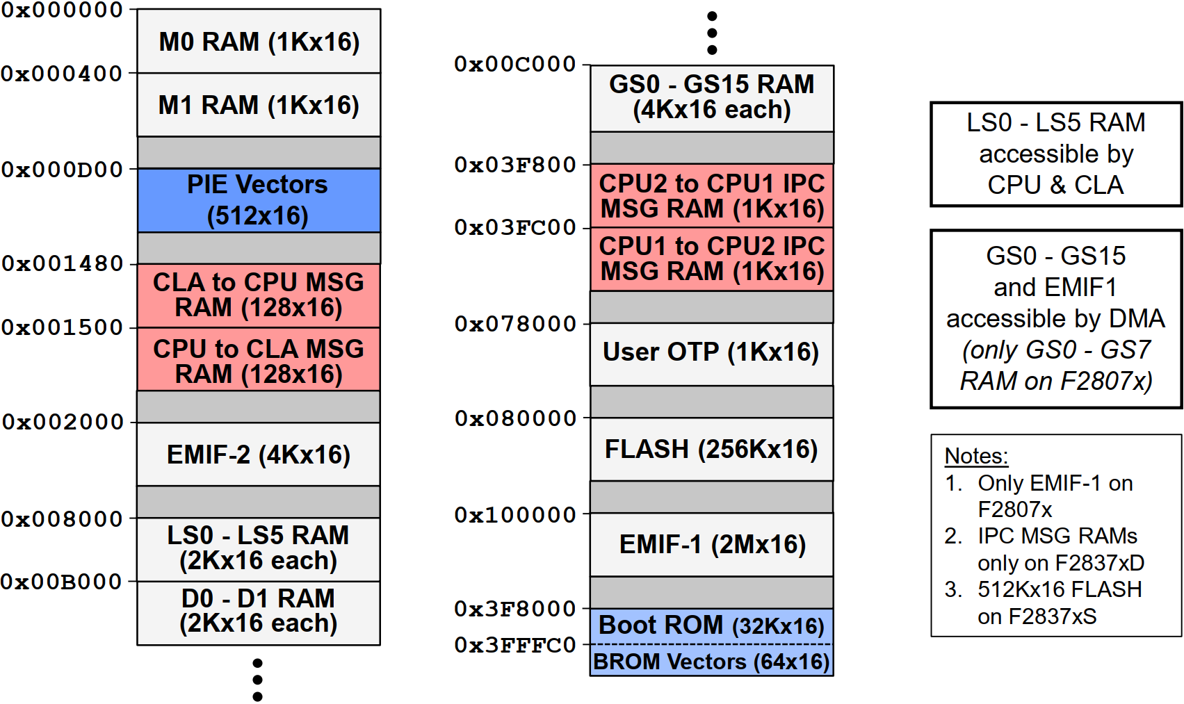
The F28x7x MCU utilizes a memory map where the unified memory blocks can be accessed in either program space, data space, or both spaces. This type of memory map lends itself well for supporting high-level programming languages. The memory structure consisting of dedicated RAM blocks, shared local RAM blocks, shared global RAM blocks, message RAM blocks, Flash, and one-time programmable (OTP) memory. The Boot is factory programmed with boot software routines and standard tables used in math related algorithms.
The C28x CPU core contains no memory, but can access on-chip and off-chip memory. The C28x uses 32-bit data addresses and 22-bit program addresses. This allows for a total address reach of 4G words (1 word = 16-bits) in data memory and 4M words in program memory.

There are four dedicated RAM block (M0, M1, D0, and D1) which are tightly coupled with the CPU, and only the CPU has access to them. The PIE Vectors are a special memory area containing the vectors for the peripheral interrupts. The six local shared memory blocks, LS0 through LS5, are accessible by its CPU and CLA. Global shared memory blocks GS0 through GS15 on the F2837x and through GS7 on the F2807x are accessible by CPU and DMA.
There are two types of message RAM blocks: CPU message RAM blocks and CLA message RAM blocks. The CPU message RAM blocks are used to share data between CPU1 subsystem and CPU2 subsystem in a dual-core device via inter-processor communications. The CLA message RAM blocks are used to share date between the CPU and CLA.
The user OTP is a one-time, programmable, memory block which contains device specific calibration data for the ADC, internal oscillators, and buffered DACs, in addition to settings used by the flash state machine for erase and program operations. Additionally, it contains locations for programming security settings, such as passwords for selectively securing memory blocks, configuring the standalone boot process, as well as selecting the boot-mode pins in case the factory-default pins cannot be used. This information is programmed into the dual code security module (DCSM). The flash memory is primarily used to store program code, but can also be used to store static data. Notice that the external memory interface is assigned a region within the memory map. The boot ROM and boot ROM vectors are located at the bottom of the memory map.
| Memory | Size | Start Address | End Address | CLA Access | DMA Access | CPU Shared |
|---|---|---|---|---|---|---|
| M0 RAM | 1K × 16 | 0x0000 0000 | 0x0000 03FF | |||
| M1 RAM | 1K × 16 | 0x0000 0400 | 0x0000 07FF | |||
| PieVectTable | 512 × 16 | 0x0000 0D00 | 0x0000 0EFF | |||
| CPUx.CLA1 to CPUx | 128 × 16 | 0x0000 1480 | 0x0000 14FF | Yes | ||
| CPUx to CPUx.CLA1 | 128 × 16 | 0x0000 1500 | 0x0000 157F | Yes | ||
| UPP TX MSG RAM | 512 × 16 | 0x0000 6C00 | 0x0000 6DFF | Yes | ||
| UPP RX MSG RAM | 512 × 16 | 0x0000 6E00 | 0x0000 6FFF | Yes | ||
| LS0 RAM | 2K × 16 | 0x0000 8000 | 0x0000 87FF | Yes | ||
| LS1 RAM | 2K × 16 | 0x0000 8800 | 0x0000 8FFF | Yes | ||
| LS2 RAM | 2K × 16 | 0x0000 9000 | 0x0000 97FF | Yes | ||
| LS3 RAM | 2K × 16 | 0x0000 9800 | 0x0000 9FFF | Yes | ||
| LS4 RAM | 2K × 16 | 0x0000 A000 | 0x0000 A7FF | Yes | ||
| LS5 RAM | 2K × 16 | 0x0000 A800 | 0x0000 AFFF | Yes | ||
| D0 RAM | 2K × 16 | 0x0000 B000 | 0x0000 B7FF | |||
| D1 RAM | 2K × 16 | 0x0000 B800 | 0x0000 BFFF | |||
| GS0 RAM | 4K × 16 | 0x0000 C000 | 0x0000 CFFF | Yes | Yes | |
| GS1 RAM | 4K × 16 | 0x0000 D000 | 0x0000 DFFF | Yes | Yes | |
| GS2 RAM | 4K × 16 | 0x0000 E000 | 0x0000 EFFF | Yes | Yes | |
| GS3 RAM | 4K × 16 | 0x0000 F000 | 0x0000 FFFF | Yes | Yes | |
| GS4 RAM | 4K × 16 | 0x0001 0000 | 0x0001 0FFF | Yes | Yes | |
| GS5 RAM | 4K × 16 | 0x0001 1000 | 0x0001 1FFF | Yes | Yes | |
| GS6 RAM | 4K × 16 | 0x0001 2000 | 0x0001 2FFF | Yes | Yes | |
| GS7 RAM | 4K × 16 | 0x0001 3000 | 0x0001 3FFF | Yes | Yes | |
| GS8 RAM | 4K × 16 | 0x0001 4000 | 0x0001 4FFF | Yes | Yes | |
| GS9 RAM | 4K × 16 | 0x0001 5000 | 0x0001 5FFF | Yes | Yes | |
| GS10 RAM | 4K × 16 | 0x0001 6000 | 0x0001 6FFF | Yes | Yes | |
| GS11 RAM | 4K × 16 | 0x0001 7000 | 0x0001 7FFF | Yes | Yes | |
| GS12 RAM | 4K × 16 | 0x0001 8000 | 0x0001 8FFF | Yes | Yes | |
| GS13 RAM | 4K × 16 | 0x0001 9000 | 0x0001 9FFF | Yes | Yes | |
| GS14 RAM | 4K × 16 | 0x0001 A000 | 0x0001 AFFF | Yes | Yes | |
| GS15 RAM | 4K × 16 | 0x0001 B000 | 0x0001 BFFF | Yes | Yes | |
| CPU2 to CPU1 RAM | 1K × 16 | 0x0003 F800 | 0x0003 FBFF | Yes | Yes | |
| CPU1 to CPU2 RAM | 1K × 16 | 0x0003 FC00 | 0x0003 FFFF | Yes | Yes | |
| CAN A MSGRAM | 2K × 16 | 0x0004 9000 | 0x0004 97FF | Yes | ||
| CAN B MSGRAM | 2K × 16 | 0x0004 B000 | 0x0004 B7FF | Yes | ||
| Flash | 256K × 16 | 0x0008 0000 | 0x000B FFFF | |||
| Secure ROM | 32K × 16 | 0x003F 0000 | 0x003F 7FFF | |||
| Boot ROM | 32K × 16 | 0x003F 8000 | 0x003F FFBF | |||
| Vectors | 64 × 16 | 0x003F FFC0 | 0x003F FFFF |
Even though pointers are 32-bits, the compiler assumes that the addresses of global variables and functions are within 22-bits.
- COFF: Common Object File Format
- EABI: Embedded Application Binary Interface
| COFF (Legacy) | EABI (Modern) | |
|---|---|---|
| char | 16 bits | 16 bits |
| enum | 16 bits | 16 bits |
| int | 16 bits | 16 bits |
| long | 32 bits | 32 bits |
| float | 32 bits | 32 bits |
| pointers | 32 bits | 32 bits |
| double | 32 bits | 64 bits |
| wchar_t | 16 bits (int) | 32 bits (long) |
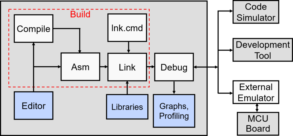
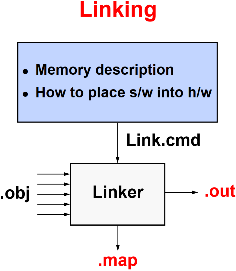
Numerous modules are joined to form a complete program by using the linker. The linker efficiently allocates the resources available on the device to each module in the system. The linker uses a command (.CMD) file to identify the memory resources and placement of where the various sections within each module are to go. Outputs of the linking process includes the linked object file (.OUT), which runs on the device, and can include a .MAP file which identifies where each linked section is located.
There are many linker options but these four handle all of the basic needs
- -o
specifies the output (executable) filename - -m
creates a map file. This file reports the linker’s results - -c tells the compiler to auto initialize your global and static variables
- -x tells the compiler to exhaustively read the libraries. Without this option libraries are searched only once, and therefore backwards references may not be resolved
To help make sense of the many compiler options, TI provides two default sets of options (configurations) in each new project you create. The Release (optimized) configuration invokes the optimizer with –o3 and disables source-level, symbolic debugging by omitting –g (which disables some optimizations to enable debug).
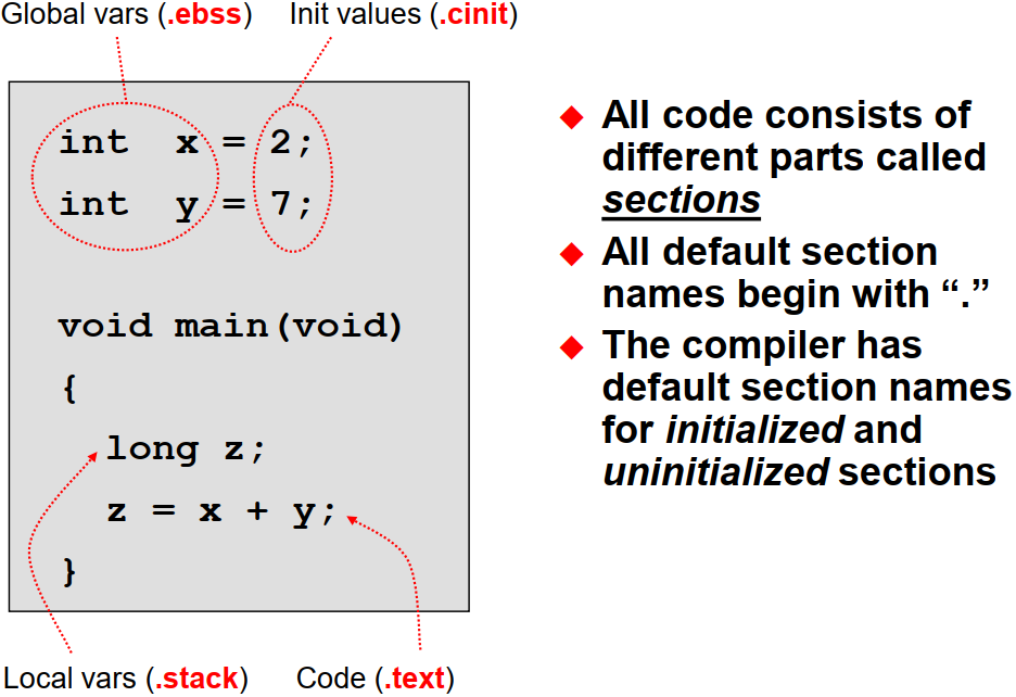
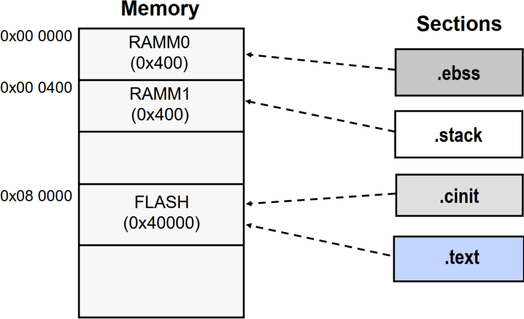
SECTIONS directive tells the linker which parts of your code and data go into which memory blocks. All default section names begin with a dot and are typically lower case. The compiler has default section names for initialized and uninitialized sections. For example, x and y are global variables, and they are placed in the section .ebss. Whereas 2 and 7 are initialized values, and they are placed in the section called .cinit. The local variables are in a section .stack, and the code is placed in a section called .txt.
Program Code (.text)
Program code consists of the sequence of instructions used to manipulate data, initialize system settings, etc. Program code must be defined upon system reset (power turn-on). Due to this basic system constraint it is usually necessary to place program code into non-volatile memory, such as FLASH or EPROM (non-volatile memory).
Constants (.cinit – initialized data)
Initialized data are those data memory locations defined at reset. It contains constants or initial values for variables. Similar to program code, constant data is expected to be valid upon reset of the system. It is often found in FLASH or EPROM (non-volatile memory).
Variables (.ebss – uninitialized data)
Uninitialized data memory locations can be changed and manipulated by the program code during runtime execution. Unlike program code or constants, uninitialized data or variables must reside in volatile memory, such as RAM. These memories can be modified and updated, supporting the way variables are used in math formulas, high-level languages, etc. Each variable must be declared with a directive to reserve memory to contain its value. By their nature, no value is assigned, instead they are loaded at runtime by the program.
| Name | Link Location | Description |
|---|---|---|
| .text | Flash | code |
| .switch | Flash | tables for switch statements |
| .cinit | Flash | init values for global and static variables |
| .data | Flash (COFF) | often empty, use .cinit instead |
| .data | Flash (EABI) | primary home for initialized global & static |
| .econst | Flash (COFF) | constants (e.g. const int k=3;) |
| .const | Flash (EABI) | constants (e.g. const int k=3;) |
| .pinit | Flash (COFF) | tables for global constructors (C++) |
| .init_array | Flash (EABI) | tables for global constructors (C++) |
| Name | Link Location | Description |
|---|---|---|
| .stack | low 64Kw RAM | local variables, function calls |
| .cio | RAM | buffer for stdio functions, printf, scanf, etc |
| .ebss | RAM (COFF) | global and static variables |
| .bss | RAM (EABI) | global and static variables |
| .heap | RAM (COFF) | near memory for malloc functions |
| .esysmem | RAM (COFF) | far memory for malloc functions |
| .sysmem | RAM (EABI) | unified memory for malloc functions |
Heap (.sysmem/.heap): --heap_size linker option
Stack (.stack): --stack_size linker option
The .init_array and .pinit sections serve the same purpose: they contain a table of pointers to constructor functions for global C++ objects.
The .sysmem and .heap represent the same thing: the memory reserved for dynamic allocation (using functions like malloc(), calloc(), or the C++ new operator).
Linking code is a three step process
- Defining the various regions of memory (on-chip RAM vs. FLASH vs. External Memory)
- Describing what sections go into which memory regions
- Running the linker with build or rebuild
MEMORY
{
PAGE 0 :  /* Program Memory: .text, .vectors, .cinit */
          /* Page 0 is reserved for the code that the processor executes */
          /* Memory (RAM/FLASH) blocks can be moved to PAGE1 for data allocation */
          /* BEGIN is used for the "boot to Flash" bootloader mode */

   BEGIN            : origin = 0x080000, length = 0x000002
   RAMM0            : origin = 0x000123, length = 0x0002DD  /* 733 x 16 */
   RAMLS05          : origin = 0x008000, length = 0x003000  /* 12k x 16 */
   RESET            : origin = 0x3FFFC0, length = 0x000002

   /* Flash sectors */
   FLASHA           : origin = 0x080002, length = 0x001FFE  /* on-chip Flash */
   FLASHB           : origin = 0x082000, length = 0x002000  /* on-chip Flash */
   FLASHC           : origin = 0x084000, length = 0x002000  /* on-chip Flash */
   FLASHD           : origin = 0x086000, length = 0x002000  /* on-chip Flash */
   FLASHE           : origin = 0x088000, length = 0x008000  /* on-chip Flash */
   FLASHF           : origin = 0x090000, length = 0x008000  /* on-chip Flash */
   FLASHG           : origin = 0x098000, length = 0x008000  /* on-chip Flash */
   FLASHH           : origin = 0x0A0000, length = 0x008000  /* on-chip Flash */
   FLASHI           : origin = 0x0A8000, length = 0x008000  /* on-chip Flash */
   FLASHJ           : origin = 0x0B0000, length = 0x008000  /* on-chip Flash */
   FLASHK           : origin = 0x0B8000, length = 0x002000  /* on-chip Flash */
   FLASHL           : origin = 0x0BA000, length = 0x002000  /* on-chip Flash */
   FLASHM           : origin = 0x0BC000, length = 0x002000  /* on-chip Flash */
   FLASHN           : origin = 0x0BE000, length = 0x001FF0  /* on-chip Flash */
// FLASHN_RSVD      : origin = 0x0BFFF0, length = 0x000010

PAGE 1 : /* Data Memory: .ebss/.bss, .stack, .sysmem */
         /* Memory (RAM/FLASH) blocks can be moved to PAGE0 for program allocation */

   BOOT_RSVD        : origin = 0x000002, length = 0x000121  /* Part of M0, BOOT rom for stack */
   RAMM1            : origin = 0x000400, length = 0x0003F8  /* 1016 x 16, on-chip RAM block M1 */
// RAMM1_RSVD       : origin = 0x0007F8, length = 0x000008

   RAMD01           : origin = 0x00B000, length = 0x001000  /* 4k x 16, for .stack */
   RAMGS015         : origin = 0x00C000, length = 0x00FFF8  /* 64k x 16 */
// RAMGS15_RSVD     : origin = 0x01BFF8, length = 0x000008

   CPU2TOCPU1RAM    : origin = 0x03F800, length = 0x000400  /* 1k x 16 */
   CPU1TOCPU2RAM    : origin = 0x03FC00, length = 0x000400  /* 1k x 16 */
}SECTIONS
{
/* Allocate program areas: */
.cinit : > FLASHA | FLASHB | FLASHC | FLASHD | FLASHE |
FLASHF | FLASHG | FLASHH | FLASHI | FLASHJ |
FLASHK | FLASHL | FLASHM | FLASHN PAGE = 0, ALIGN(8)
.text : >> FLASHA | FLASHB | FLASHC | FLASHD | FLASHE |
FLASHF | FLASHG | FLASHH | FLASHI | FLASHJ |
FLASHK | FLASHL | FLASHM | FLASHN PAGE = 0, ALIGN(8)
codestart : > BEGIN PAGE = 0, ALIGN(8)
/* Allocate uninitalized data sections: */
.stack : > RAMD01 | RAMM1, PAGE = 1
// Allocate memory for customized varibale and array
.my_arrs : > RAMGS015, PAGE = 1
.my_vars : > RAMGS015, PAGE = 1
.switch : > FLASHA | FLASHB | FLASHC | FLASHD | FLASHE |
FLASHF | FLASHG | FLASHH | FLASHI | FLASHJ |
FLASHK | FLASHL | FLASHM | FLASHN PAGE = 0, ALIGN(8)
.reset : > RESET, PAGE = 0, TYPE = DSECT /* not used */
#if defined(__TI_EABI__)
.init_array : > FLASHA | FLASHB | FLASHC | FLASHD | FLASHE |
FLASHF | FLASHG | FLASHH | FLASHI | FLASHJ |
FLASHK | FLASHL | FLASHM | FLASHN, PAGE = 0, ALIGN(8)
.bss : > RAMGS015, PAGE = 1
.bss:output : > RAMLS05, PAGE = 0
.bss:cio : > RAMGS015, PAGE = 1
.data : > RAMGS015, PAGE = 1
.sysmem : > RAMGS015, PAGE = 1
/* Initalized sections go in Flash */
.const : > FLASHA | FLASHB | FLASHC | FLASHD | FLASHE |
FLASHF | FLASHG | FLASHH | FLASHI | FLASHJ |
FLASHK | FLASHL | FLASHM | FLASHN, PAGE = 0, ALIGN(8)
#else
.pinit : > FLASHA | FLASHB | FLASHC | FLASHD | FLASHE |
FLASHF | FLASHG | FLASHH | FLASHI | FLASHJ |
FLASHK | FLASHL | FLASHM | FLASHN, PAGE = 0, ALIGN(8)
.ebss : >> RAMGS015, PAGE = 1
.esysmem : > RAMGS015, PAGE = 1
.cio : > RAMGS015, PAGE = 1
/* Initalized sections go in Flash */
.econst : >> FLASHA | FLASHB | FLASHC | FLASHD | FLASHE |
FLASHF | FLASHG | FLASHH | FLASHI | FLASHJ |
FLASHK | FLASHL | FLASHM | FLASHN PAGE = 0, ALIGN(8)
#endif
FFT_buffer_1 : >> RAMGS015, ALIGN = FFT_ALIGN
FFT_buffer_2 : >> RAMGS015
FPUmathTables : >> RAMGS015
FPUfftTables : >> RAMGS015
FpuRegsFile : >> RAMGS015
#ifdef __TI_COMPILER_VERSION__
#if __TI_COMPILER_VERSION__ >= 15009000
#if defined(__TI_EABI__)
.TI.ramfunc : {} LOAD = FLASHA | FLASHB | FLASHC | FLASHD | FLASHE |
FLASHF | FLASHG | FLASHH | FLASHI | FLASHJ |
FLASHK | FLASHL | FLASHM | FLASHN,
RUN = RAMLS05,
LOAD_START(RamfuncsLoadStart),
LOAD_SIZE(RamfuncsLoadSize),
LOAD_END(RamfuncsLoadEnd),
RUN_START(RamfuncsRunStart),
RUN_SIZE(RamfuncsRunSize),
RUN_END(RamfuncsRunEnd),
PAGE = 0, ALIGN(8)
#else
.TI.ramfunc : {} LOAD = FLASHA | FLASHB | FLASHC | FLASHD | FLASHE |
FLASHF | FLASHG | FLASHH | FLASHI | FLASHJ |
FLASHK | FLASHL | FLASHM | FLASHN,
RUN = RAMLS05,
LOAD_START(_RamfuncsLoadStart),
LOAD_SIZE(_RamfuncsLoadSize),
LOAD_END(_RamfuncsLoadEnd),
RUN_START(_RamfuncsRunStart),
RUN_SIZE(_RamfuncsRunSize),
RUN_END(_RamfuncsRunEnd),
PAGE = 0, ALIGN(8)
#endif
#else
ramfuncs : LOAD = FLASHA | FLASHB | FLASHC | FLASHD | FLASHE |
FLASHF | FLASHG | FLASHH | FLASHI | FLASHJ |
FLASHK | FLASHL | FLASHM | FLASHN,
RUN = RAMLS05,
LOAD_START(_RamfuncsLoadStart),
LOAD_SIZE(_RamfuncsLoadSize),
LOAD_END(_RamfuncsLoadEnd),
RUN_START(_RamfuncsRunStart),
RUN_SIZE(_RamfuncsRunSize),
RUN_END(_RamfuncsRunEnd),
PAGE = 0, ALIGN(8)
#endif
#endif
/* The following section definitions are required when using the IPC API Drivers */
GROUP : > CPU1TOCPU2RAM, PAGE = 1
{
PUTBUFFER
PUTWRITEIDX
GETREADIDX
}
GROUP : > CPU2TOCPU1RAM, PAGE = 1
{
GETBUFFER : TYPE = DSECT
GETWRITEIDX : TYPE = DSECT
PUTREADIDX : TYPE = DSECT
}
}
[1]
TMS320F2837xD Microcontroller Workshop
[2]
C28x Memory Map
[3]
TI Linker Command File Primer
[4]
A Primer on Linker Scripts and Command Files
[5]
C2000 SysConfig Linker Command Tool
Back to top of the page