
- General Purpose Digital I/O
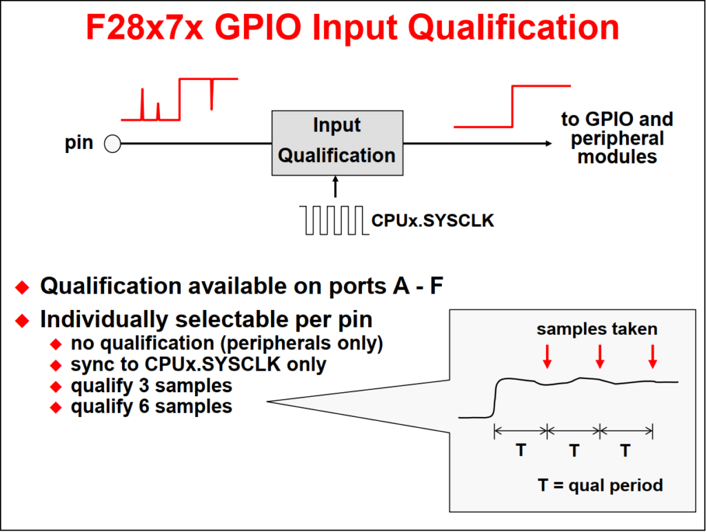
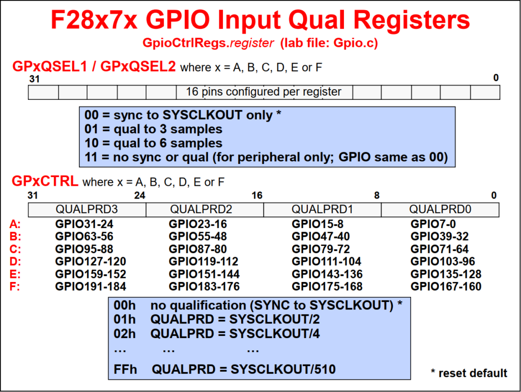
- GPIO Input Qualification
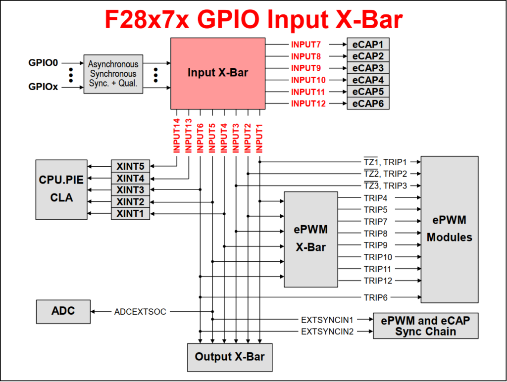
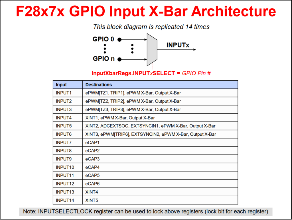
- GPIO Input X-Bar
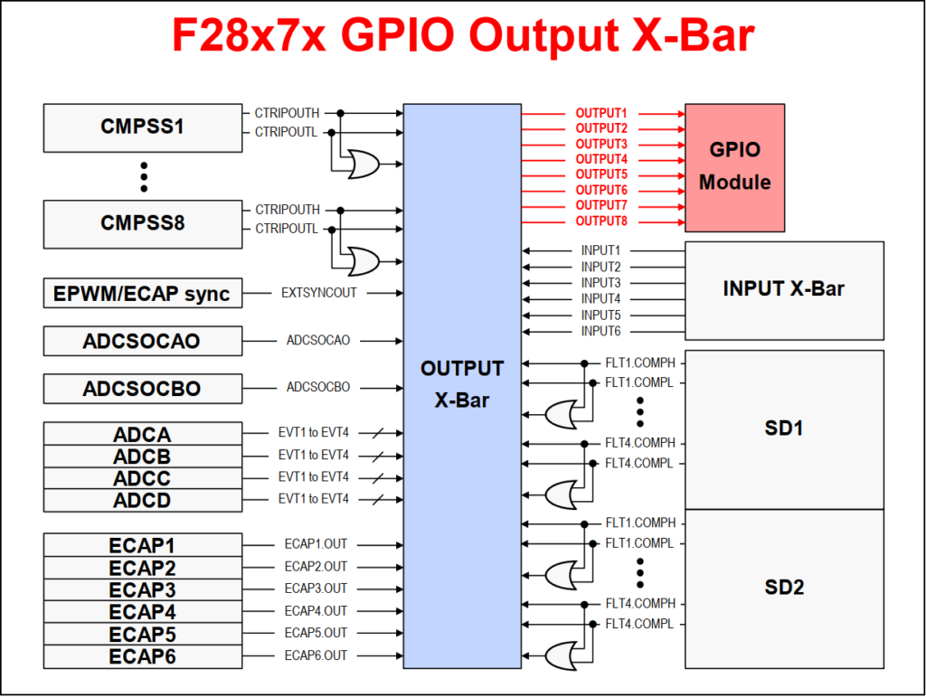
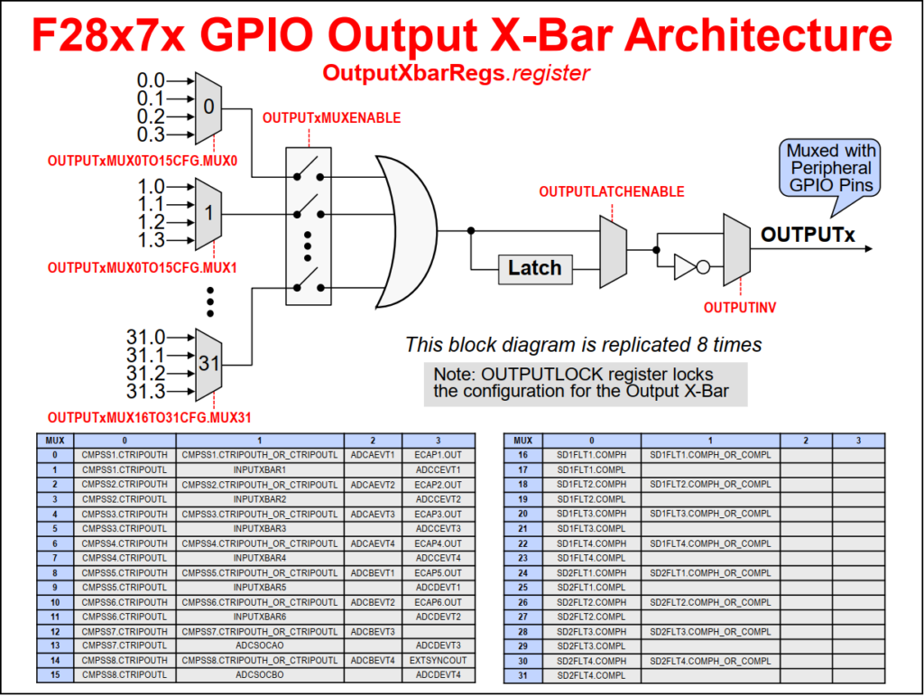
- GPIO Output X-Bar
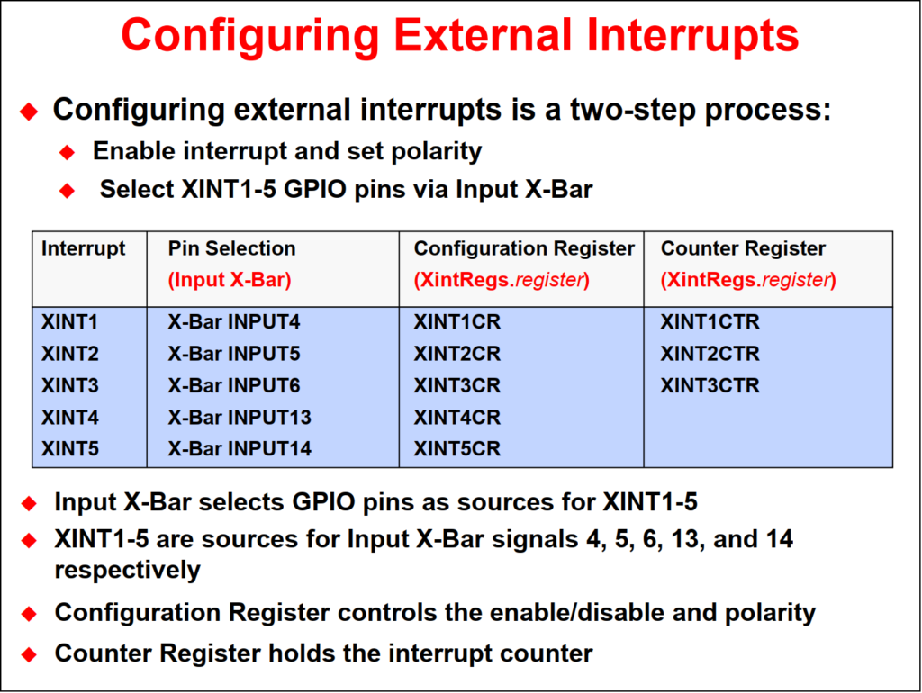
- External Interrupts
- Example: GPIO Bitfield & Driverlib
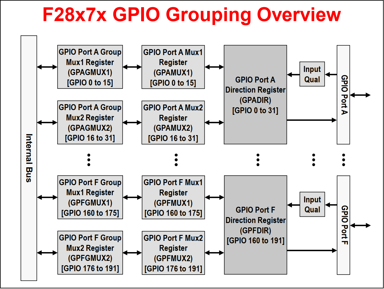
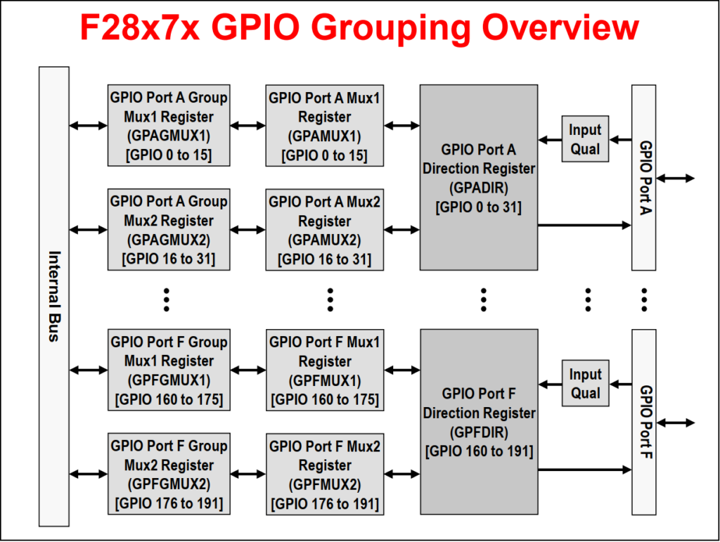
The F2837xD device incorporates a multiplexing scheme to enable each I/O pin to be configured as a GPIO pin or one of several peripheral I/O signals. Sharing a pin across multiple functions maximizes application flexibility while minimizing package size and cost. A GPIO Group multiplexer and four GPIO Index multiplexers provide a double layer of multiplexing to allow up to twelve independent peripheral signals and a digital I/O function to share a single pin.
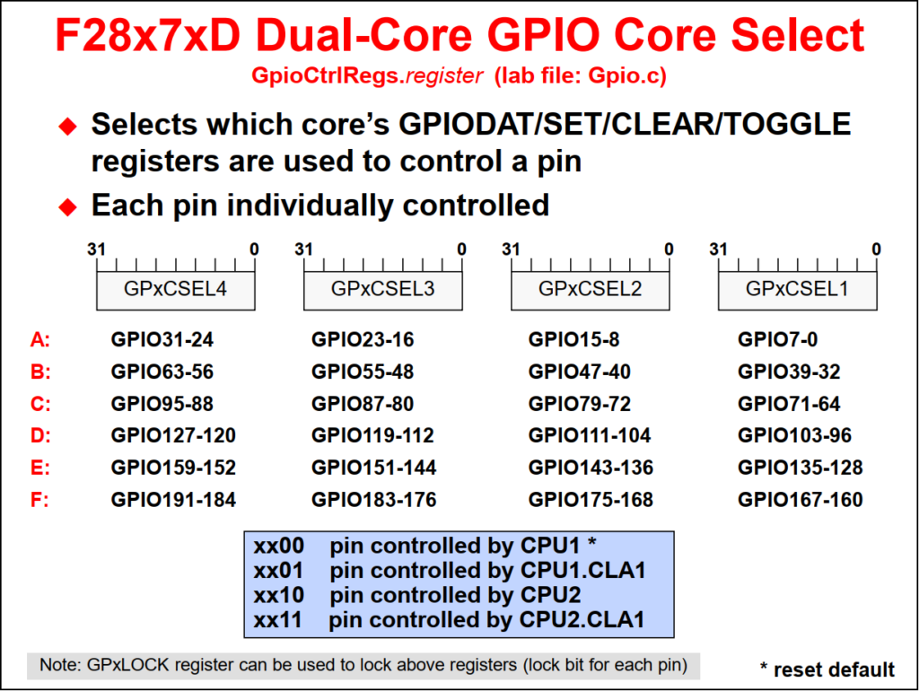
Each output pin can be controlled by either a peripheral or CPU1, CPU1 CLA, CPU2, or CPU2 CLA. However, the peripheral multiplexing and pin assignment can only be configured by CPU1. By default, all of the pins are configured as GPIO, and when configured as a signal input pin, a qualification sampling period can be specified to remove unwanted noise. Optionally, each pin has an internal pullup resistor that can be enabled in order to keep the input pin in a known state when no external signal is driving the pin.
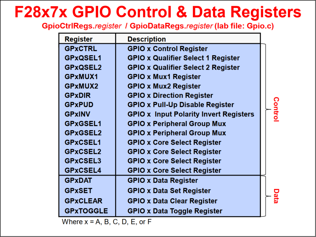
The I/O pins are grouped into six ports, and each port has 32 pins except for the sixth port which has nine pins (i.e. the remaining I/O pins). For a GPIO, each port has a series of registers that are used to control the value on the pins, and within these registers each bit corresponds to one GPIO pin.
If the pin is configured as GPIO, a direction (DIR) register is used to specify the pin as either an input or output. By default, all GPIO pins are inputs. The current state of a GPIO pin corresponds to a bit value in a data (DAT) register, regardless if the pin is configured as GPIO or a peripheral function. Writing to the DAT register bit field clears or sets the corresponding output latch, and if the pin is configured as an output the pin will be driven either low or high. The state of various GPIO output pins on the same port can be easily modified using the SET, CLEAR, and TOGGLE registers. The advantage of using these registers is a single instruction can be used to modify only the pins specified without disturbing the other pins. This also eliminates any timing issues that may occur when writing directly to the data registers.
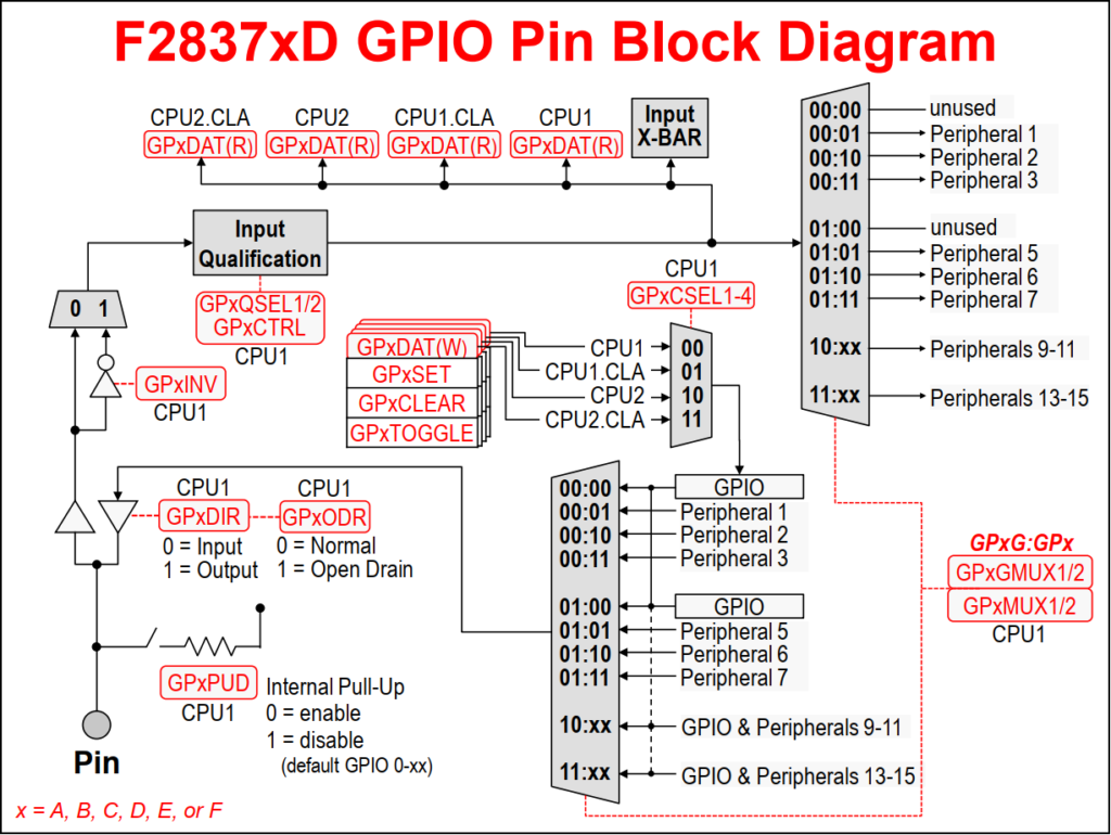
The input qualification scheme is very flexible, and the type of input qualification can be configured for each GPIO pin individually. In the case of a GPIO input pin, the qualification can be specified as only synchronize to SYSCLKOUT or qualification by a sampling window. For pins that are configured as peripheral inputs, the input can also be asynchronous in addition to synchronized to SYSCLKOUT or qualified by a sampling window.
The Input X-BAR is used to route external GPIO signals into the device. It has access to every GPIO pin, where each signal can be routed to any or multiple destinations which include the ADCs, eCAPs, ePWMs, Output X-BAR, and external interrupts. This provides additional flexibility above the multiplexing scheme used by the GPIO structure. Since the GPIO does not affect the Input X-BAR, it is possible to route the output of one peripheral to another, such as measuring the output of an ePWM with an eCAP for frequency testing.
The Output X-BAR is used to route various internal signals out of the device. It contains eight outputs that are routed to the GPIO structure, where each output has one or multiple assigned pin positions, which are labeled as OUTPUTXBARx. Additionally, the Output X-BAR can select a single signal or logically OR up to 32 signals.
- Five external interrupt signals: XINT1, XINT2, XINT3, XINT4 and XINT5
- Each can be mapped to any of GPIO pins via the X-Bar Input architecture
- XINT1, XINT2 and XINT3 also each have a free-running 16-bit counter that measures the elapsed time between interrupts. The counter resets to zero each time the interrupt occurs
#include "F28x_Project.h"

// F2837xD_Gpio_defines.h
#define GPIO_MUX_CPU1       0x0
#define GPIO_MUX_CPU1CLA    0x1
#define GPIO_MUX_CPU2       0x2
#define GPIO_MUX_CPU2CLA    0x3

#define GPIO_INPUT          0
#define GPIO_OUTPUT         1
#define GPIO_PUSHPULL       0
#define GPIO_PULLUP         (1 << 0)
#define GPIO_INVERT         (1 << 1)
#define GPIO_OPENDRAIN      (1 << 2)
#define GPIO_SYNC           (0x0 << 4)
#define GPIO_QUAL3          (0x1 << 4)
#define GPIO_QUAL6          (0x2 << 4)
#define GPIO_ASYNC          (0x3 << 4)

// CPU1 output
GPIO_SetupPinMux(31, GPIO_MUX_CPU1, 0);
GPIO_SetupPinOptions(31, GPIO_OUTPUT, 0);
GPIO_SetupPinOptions(31, GPIO_OUTPUT, GPIO_PUSHPULL);

// CPU1 input
GPIO_SetupPinMux(14, GPIO_MUX_CPU1, 0);
GPIO_SetupPinOptions(14, GPIO_INPUT, 0);

// CPU1 pushbutton
GPIO_SetupPinMux(122, GPIO_MUX_CPU1, 0);
GPIO_SetupPinOptions(122, GPIO_INPUT, GPIO_PULLUP);

// CPU2 output
GPIO_SetupPinMux(34, GPIO_MUX_CPU2, 0);
GPIO_SetupPinOptions(34, GPIO_OUTPUT, 0);
GPIO_SetupPinOptions(34, GPIO_OUTPUT, GPIO_PUSHPULL);

// CPU2 input
GPIO_SetupPinMux(10, GPIO_MUX_CPU2, 0);
GPIO_SetupPinOptions(10, GPIO_INPUT, 0);

GPIO_WritePin(31, 0)
GPIO_WritePin(31, 1)

uint16_t state;
state = GPIO_ReadPin(14);

EALLOW;

// CPU1 output
GpioCtrlRegs.GPAGMUX2.bit.GPIO31 = 0; // Select GPIO group mux
GpioCtrlRegs.GPAMUX2.bit.GPIO31  = 0; // Select GPIO function
GpioCtrlRegs.GPAODR.bit.GPIO31   = 0; // Normal output, not open-drain = push-pull
GpioCtrlRegs.GPADIR.bit.GPIO31   = 1; // GPIO31 = output

// CPU1 input
// For a normal GPIO input, use the pull-up only if you need a default HIGH level
GpioCtrlRegs.GPAGMUX1.bit.GPIO14 = 0; // GPIO group mux = GPIO
GpioCtrlRegs.GPAMUX1.bit.GPIO14  = 0; // GPIO mux = GPIO
GpioCtrlRegs.GPAPUD.bit.GPIO14   = 0; // Enable pull-up
GpioCtrlRegs.GPADIR.bit.GPIO14   = 0; // Input

// CPU2 output
GpioCtrlRegs.GPBGMUX1.bit.GPIO34 = 0; // Select GPIO group mux
GpioCtrlRegs.GPBMUX1.bit.GPIO34  = 0; // Select GPIO function
GpioCtrlRegs.GPBCSEL1.bit.GPIO34 = 2; // MUX with CPU2
GpioCtrlRegs.GPBODR.bit.GPIO34   = 0; // Normal output, not open-drain = push-pull
GpioCtrlRegs.GPBDIR.bit.GPIO34   = 1; // GPIO34 = output

// CPU2 input
// For a normal GPIO input, use the pull-up only if you need a default HIGH level
GpioCtrlRegs.GPAGMUX1.bit.GPIO10 = 0; // GPIO group mux = GPIO
GpioCtrlRegs.GPAMUX1.bit.GPIO10  = 0; // GPIO mux = GPIO
GpioCtrlRegs.GPAPUD.bit.GPIO10   = 0; // Enable pull-up
GpioCtrlRegs.GPADIR.bit.GPIO10   = 0; // Input
GpioCtrlRegs.GPACSEL2.bit.GPIO10 = 2; // Mux with CPU2

EDIS;

GpioDataRegs.GPBSET.bit.GPIO31 = 1;
GpioDataRegs.GPBSET.bit.GPIO34 = 1;

GpioDataRegs.GPBCLEAR.bit.GPIO31 = 1;
GpioDataRegs.GPBCLEAR.bit.GPIO34 = 1;

GpioDataRegs.GPATOGGLE.bit.GPIO31 = 1;
GpioDataRegs.GPATOGGLE.bit.GPIO34 = 1;

uint16_t state;
state = GpioDataRegs.GPADAT.bit.GPIO14;
state = GpioDataRegs.GPADAT.bit.GPIO10;
#include "driverlib.h"
#include "device.h"
#define GPIO_PIN_TYPE_STD 0x0000U // Push-pull output or floating input
#define GPIO_PIN_TYPE_PULLUP 0x0001U // Pull-up enable for input
#define GPIO_PIN_TYPE_INVERT 0x0002U // Invert polarity on input
#define GPIO_PIN_TYPE_OD 0x0004U // Open-drain on output
// CPU1 output
GPIO_setPadConfig(15UL, GPIO_PIN_TYPE_STD);
GPIO_setDirectionMode(15UL, GPIO_DIR_MODE_OUT);
GPIO_setMasterCore(15UL, GPIO_CORE_CPU1);
// CPU1 input
GPIO_setPadConfig(14UL, GPIO_PIN_TYPE_STD);
GPIO_setDirectionMode(14UL, GPIO_DIR_MODE_IN);
GPIO_setMasterCore(14UL, GPIO_CORE_CPU1);
// CPU2 output
GPIO_setPadConfig(10UL, GPIO_PIN_TYPE_STD);
GPIO_setDirectionMode(10UL, GPIO_DIR_MODE_OUT);
GPIO_setMasterCore(10UL, GPIO_CORE_CPU2);
// CPU2 input
GPIO_setPadConfig(11UL, GPIO_PIN_TYPE_STD);
GPIO_setDirectionMode(11UL, GPIO_DIR_MODE_IN);
GPIO_setMasterCore(11UL, GPIO_CORE_CPU2);
GPIO_writePin(15UL, 0);
GPIO_writePin(15UL, 1);
GPIO_togglePin(15UL);
GPIO_togglePin(10UL);
state = GPIO_readPin(14UL);
state = GPIO_readPin(11UL);Back to top of the page