
- TMS320F28x7x Inter-Processor Communications (IPC)
- TMS320F28x7x IPC Global Shared RAM
- TMS320F28x7x IPC Message RAM
- TMS320F28x7x IPC Message Registers
- TMS320F28x7x IPC Interrupts and Flags
- TMS320F28x7x IPC Data Transfer
- TMS320F28x7x IPC Software Solutions Summary
The IPC allows communication between the two CPU subsystems (i.e. CPU1 and CPU2).
- Message RAMs
- IPC flags and interrupts
- IPC command registers
- Flash pump semaphore
- Clock configuration semaphore
- Free-running counter
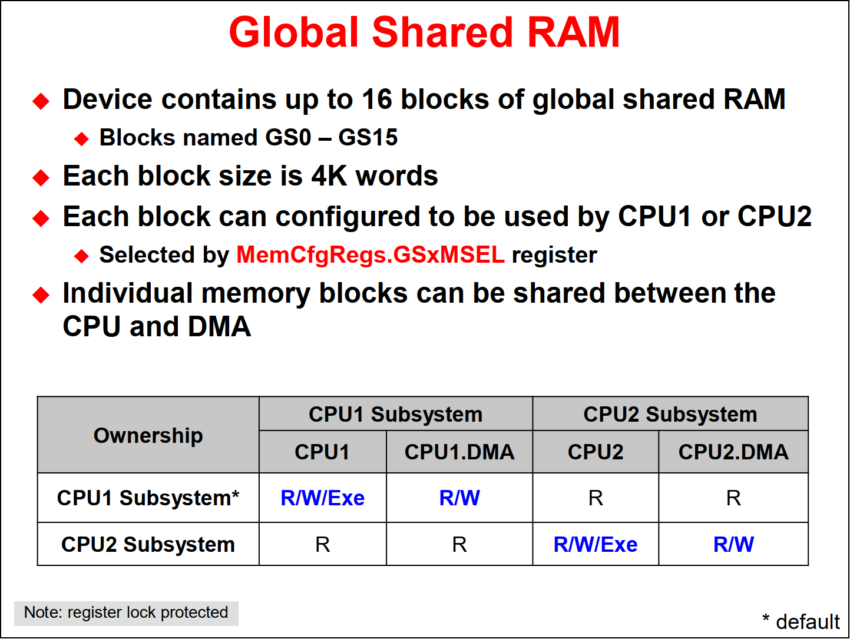
There are up to 16 blocks of shared RAM on F2837xD devices. These shared RAM blocks are typically used by the application, but can also be used for transferring messages and data. Each block can individually be owned by either CPU1 or CPU2.
CPU1 core ownership:
At reset, CPU1 owns all of the shared RAM blocks. In this configuration CPU1 core can freely use the memory blocks. CPU1 can read, write or execute from the block and CPU1.DMA can read or write. On the CPU2 core, CPU2 and CPU2.DMA can only read from these blocks. Blocks owned by the CPU1 core can be used by the CPU1 to send CPU2 messages. This is referred to as C1toC2.
CPU2 core ownership:
After reset, the CPU1 application can assign ownership of blocks to the CPU2 subsystem. In this configuration, CPU2 core can freely use the blocks. CPU2 can read, write or execute from the block and the CPU2.DMA can read or write. CPU1 core, however can only read from the block. Blocks owned by CPU2 core can be used can be used to send messages from the CPU2 to CPU1. This is referred to as C2toC1.

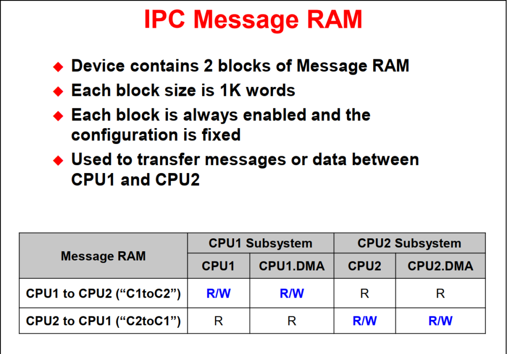
The F2837xD has two dedicated message RAM blocks. Each block is 1K words in length. Unlike the shared RAM blocks, these blocks provide communication in one direction only and cannot be reconfigured.
CPU1 to CPU2 C1toC2 message RAM:
The first message RAM is the CPU1 to CPU2 or C1toC2. This block can be read or written to by the CPU1 and read by the CPU2. CPU1 can write a message to this block and then the CPU2 can read it.
CPU2 to CPU1 C2toC1 message RAM:
The second message RAM is the CPU2 to CPU1 or C2toC1. This block can be read or written to by CPU2 and read by CPU1. This means CPU2 can write a message to this block and then CPU1 can read it. After the sending CPU writes a message it can inform the receiver CPU that it is available through an interrupt or flag.
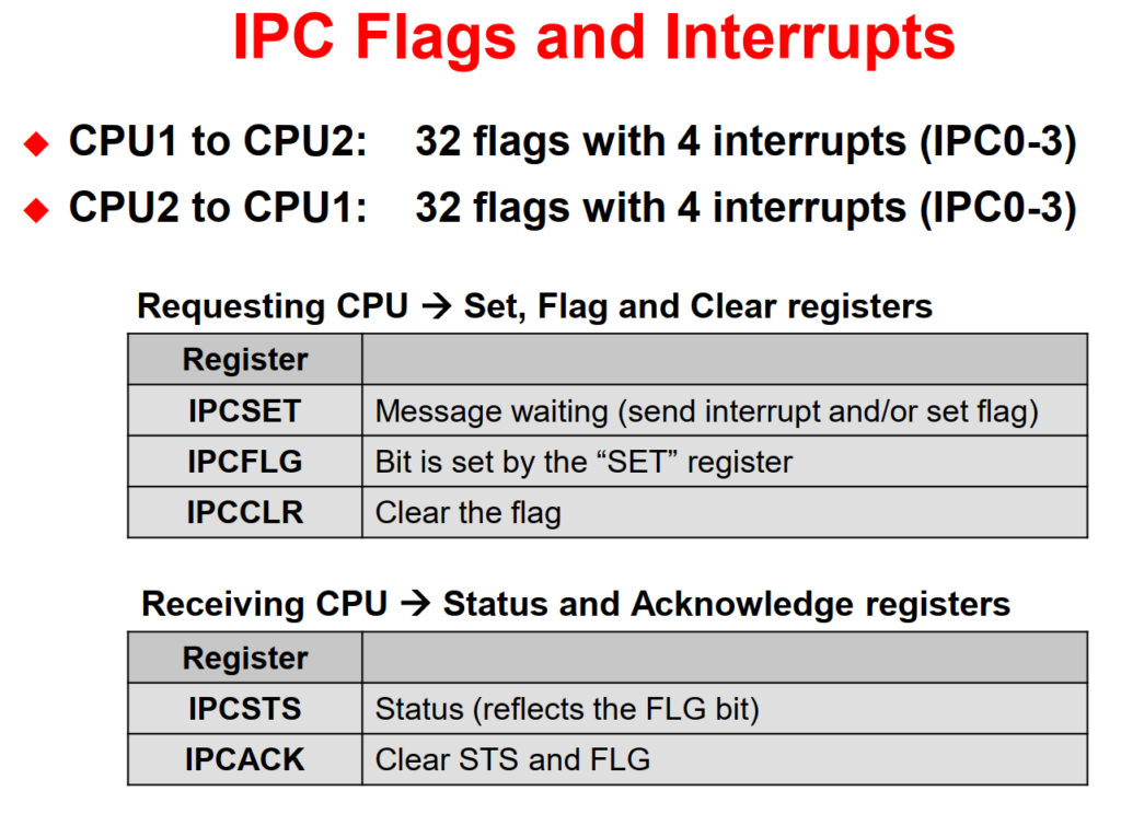
When the sending CPU wants to inform the receiver that a message is ready, it can make use of an interrupt or flag. There are identical IPC interrupt and flag resources on both CPU1 core and CPU2 core.
4 Interrupts:
There are 4 interrupts that CPU1 can send to CPU2 (and vice-versa) through the Peripheral Interrupt Expansion (PIE) module. Each of the interrupts has a dedicated vector within the PIE, IPC0 – IPC3.
28 Flags:
In addition, there are 28 flags available to each of the CPU cores. These flags can be used for messages that are not time critical or they can be used to send status back to originating processor. The flags and interrupts can be used however the application sees fit and are not tied to particular operation in hardware.
Registers: Set, Flag, Clear, Status and Acknowledge
The registers to control the IPC interrupts and flags are 32-bits:
- Bits [3:0] = interrupt & flag
- Bits [31:4] = flag only
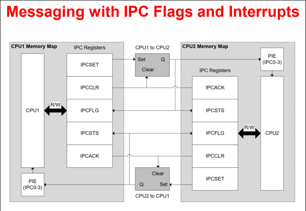
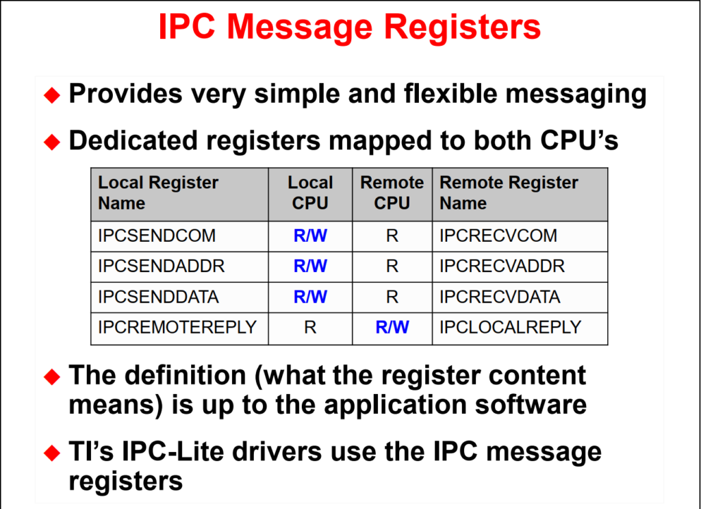
The F2837xD IPC is very easy to use. At the most basic level, the application does not need any separate software drivers to communicate between processors. It can utilize the message RAM’s and shared RAM blocks to pass data between processors at a fixed address known to both processors. Then the sending processor can use the IPC flag registers merely to flag to the receiving processor that the data is ready. Once the receiving processor has grabbed the data, it will then acknowledge the corresponding IPC flag to indicate that it is ready for more messages.
As an example:
- CPU1 would write a message to the CPU2 in C1toC2 MSG RAM.
- The CPU1 would write a 1 to the appropriate flag bit in the C1TOC2IPCSET register. This sets the C1TOC2IPCFLG, which also sets the C1TOC2IPCSTS register on CPU2, letting CPU2 know that a message is available.
- CPU2 sees that a bit in the C1TOC2IPCSTS register is set.
- CPU2 reads the message from the C1toC2 MSG RAM and then
- It writes a 1 to the same bit in the C1TOC2IPCACK register to acknowledge that it has received the message. This subsequently clears the flag bit in C1TOC2IPCFLG and C1TOC2IPCSTS.
- CPU1 can then send more messages using that particular flag bit.